

Intermetallic Compound Formation Begins the Moment Molten Solder Meets Bare Copper
In surface mount technology, a reliable solder joint is far more than two metals pressed together. The instant molten solder touches an exposed copper pad during reflow soldering, atoms from both sides begin to diffuse across the boundary and form a new crystalline structure called an intermetallic compound, or IMC. This intermetallic compound formation is not a defect. It is the chemical reaction that actually bonds the component lead to the printed circuit board. Without it, the joint would simply fall apart. Yet the same intermetallic compound that creates the bond can also undermine solder joint reliability when it grows too thick or too thin. For any PCB assembly manufacturer, understanding where this thin reaction layer comes from is the first step toward controlling it.

The Cu6Sn5 and Cu3Sn Layers Define Solder Joint Reliability in SMT Assembly
When tin-based solder reacts with copper, two intermetallic compounds appear in a predictable stack. Closest to the bulk solder sits the Cu6Sn5 phase, a fine-grained layer that forms quickly and provides most of the mechanical anchoring. Closer to the copper itself sits Cu3Sn, a slower-growing, more brittle phase that appears only after extended heating. Together these two layers make up the intermetallic compound zone at every solder joint. Their combined thickness, typically measured in micrometres, is one of the strongest predictors of solder joint reliability in SMT assembly. A joint with too little intermetallic compound has not fully wet the pad, while a joint with an oversized layer becomes brittle and prone to cracking under thermal stress.

Reflow Soldering Process Parameters Control Intermetallic Compound Thickness at the Interface
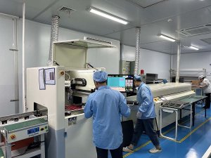
The reflow soldering process is where intermetallic compound formation is set in stone. Peak temperature and time above liquidus are the two dominant variables. A higher peak and a longer soak give tin and copper more time to react, thickening the intermetallic compound layer. A well-optimized reflow profile keeps the board just long enough above 217 degrees Celsius, the melting point of SAC305, to wet fully, then cools quickly to limit further growth. Experienced process engineers tune the reflow soldering process so that the intermetallic compound reaches a target of roughly one to four micrometres. Thick enough to bond, thin enough to stay ductile. Double reflow, where a board passes through the oven twice for double-sided assembly, naturally produces a thicker intermetallic compound on the first-side joints and must be accounted for in the profile design.
Thermal Aging Grows the Intermetallic Compound and Weakens Long-Term Solder Joint Reliability
Intermetallic compound formation does not stop when the board leaves the oven. During field operation, especially in applications that see temperature swings, the joint continues to age. The Cu3Sn layer in particular keeps growing as copper diffuses into the tin, consuming the ductile solder and leaving behind a thicker, harder intermetallic compound zone. After hundreds of thermal cycles, this growth can push solder joint reliability downward, leading to intermittent failures in connectors, ball-grid arrays, and power components. Accelerated life testing that subjects assemblies to repeated thermal cycling is the standard way a PCB assembly manufacturer proves that intermetallic compound growth will stay within safe limits for the intended service life of the product.
Nickel Barrier Layers Change Intermetallic Compound Formation on ENIG Surface Finishes
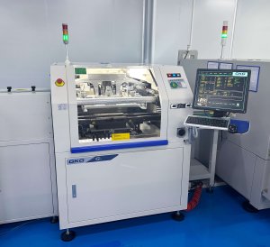
Surface finish selection changes the chemistry of the interface. On an ENIG, electroless nickel immersion gold, board, the solder does not meet copper directly. It meets a nickel barrier capped with a thin gold layer that dissolves during reflow. The resulting intermetallic compound is Ni3Sn4 rather than Cu6Sn5, and its growth rate differs from the copper system. This nickel-based intermetallic compound formation is generally more stable under thermal aging, which is one reason ENIG is favored for fine-pitch and wire-bondable pads. However, a black-pad defect, caused by excessive phosphorus enrichment at the nickel surface, can sabotage the intermetallic compound and ruin solder joint reliability, so finish quality control remains essential.
Excessive Intermetallic Compound Growth Causes Kirkendall Voids and Brittle Solder Joints
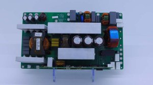
When intermetallic compound formation runs out of control, the microstructure develops problems that directly threaten the assembly. One well-documented failure is the Kirkendall void, a chain of tiny cavities that appears at the Cu3Sn interface as copper atoms diffuse faster than tin atoms, leaving behind empty space. These voids act as crack initiation sites. A second issue is simple brittleness. A joint that is mostly intermetallic compound behaves like ceramic rather than metal, snapping instead of bending under mechanical shock. Both mechanisms explain why over-aged or over-reflowed boards can pass initial inspection yet fail solder joint reliability testing weeks later. Keeping the intermetallic compound thin through correct process windows is the primary defense.
Process Controls Reduce Intermetallic Compound Risk During High-Volume PCB Assembly
High-volume production makes consistency the hard part. The following controls help keep intermetallic compound formation inside the safe window on every board:
- Verify pad copper finish and surface preparation before solder paste printing so bare copper is clean and oxide-free.
- Lock the reflow soldering process recipe and audit peak temperature and time above liquidus on every oven zone daily.
- Minimize unnecessary thermal excursions by combining placement and reflow steps and avoiding redundant rework heating.
- Qualify double-reflow boards with cross-section analysis to confirm the first-side intermetallic compound stays below the limit.
- Store moisture-sensitive parts correctly so that popcorning and extra rework cycles do not add uncontrolled reflow time.
- Sample and cross-section joints from the first article and at fixed intervals to track intermetallic compound growth trends.
A partner offering a one-stop PCBA solution can fold all of these checks into a single documented process flow, which is far easier to hold consistent than handing the steps to several vendors.
X-Ray and Cross-Section Analysis Verify Intermetallic Compound Formation in Production
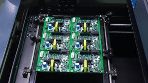
You cannot manage what you cannot measure. While automated optical inspection confirms that a joint is present, it cannot see the intermetallic compound buried inside. The definitive check is a polished cross-section. A lab grinds the joint, etches it, and images the interface so the intermetallic compound layers can be measured directly. For hidden joints such as ball-grid arrays, 2D or 3D X-ray inspection infers voiding and bonding quality that correlates with intermetallic compound health. The table below summarizes how the common interface layers compare:
| Interface Layer | Chemical Phase | Location | Primary Growth Driver |
|---|---|---|---|
| Near-solder IMC | Cu6Sn5 | Between solder and Cu3Sn | Reflow peak and soak time |
| Near-copper IMC | Cu3Sn | Between Cu6Sn5 and copper | Thermal aging over time |
| Nickel-system IMC | Ni3Sn4 | On ENIG nickel barrier | Nickel diffusion during reflow |
| Brittle failure zone | Overgrown IMC | Whole interface | Excess heat and double reflow |
By pairing routine cross-section audits with a stable reflow soldering process, a competent PCB assembly manufacturer keeps intermetallic compound formation predictable and solder joint reliability high across the full production run.
Summary
Intermetallic compound formation is the chemical reaction that actually bonds every SMT solder joint, and its thickness is one of the strongest predictors of solder joint reliability. The Cu6Sn5 and Cu3Sn layers grow during reflow and continue to thicken with thermal aging, so controlling peak temperature, time above liquidus, and unnecessary rework is essential. With the right process windows, surface-finish choices, and cross-section verification, intermetallic compound growth stays in the safe range and long-term PCB assembly performance is protected.

FAQ
What exactly is an intermetallic compound in a solder joint?
An intermetallic compound is a brittle metallic alloy that forms at the boundary between molten tin-based solder and the underlying copper or nickel pad during reflow soldering. It is the layer that physically bonds the component to the board, and its thickness must be controlled to protect solder joint reliability.
Why does the intermetallic compound keep growing after assembly?
Even after the board cools, copper and tin atoms continue to diffuse at the interface during field operation, especially under temperature changes. This thermal aging slowly thickens the Cu3Sn layer, which is why accelerated thermal cycling tests are used to confirm long-term solder joint reliability.
How thick should the intermetallic compound layer be?
Most SMT assembly standards target a combined intermetallic compound thickness in the range of roughly one to four micrometres. Below this, wetting may be incomplete. Above it, the joint becomes brittle and vulnerable to cracking, so the reflow soldering process is tuned to stay inside the window.
Does ENIG surface finish change the intermetallic compound?
Yes. On an ENIG finish the solder reacts with the nickel barrier instead of copper, forming Ni3Sn4 rather than Cu6Sn5. This nickel-based intermetallic compound formation is generally more stable under aging, though poor nickel quality can cause black-pad defects that ruin the joint.
Can too much intermetallic compound be fixed after reflow?
No. Once the intermetallic compound has overgrown, the joint cannot be restored by simple adjustment. The board would need rework or scrap. The only effective control is preventing excess growth in the first place through a locked, audited reflow soldering process.
How do factories verify intermetallic compound formation?
The reliable method is a polished cross-section analyzed under a microscope, which measures the IMC layers directly. For hidden ball-grid joints, 2D or 3D X-ray inspection is used to infer bonding quality, and routine sampling tracks intermetallic compound trends across the production run.