
The PCBA (Printed Circuit Board Assembly) field encompasses a rich system of specialized terminology covering core processes such as substrate manufacturing, assembly workflows, and quality inspection. This article systematically outlines the definitions and technical implications of key terms like copper foil, etching, and reflow soldering, helping practitioners quickly master industry language and enhance professional communication efficiency.
1.PCB Substrate Materials and Fundamental Process Terminology
1.1 Copper Foil
Copper foil serves as the core conductive layer material for PCBs, manufactured through rolling or electrolytic processes. Its thickness ranges from 1/3 oz to 10 oz, corresponding to 12 microns to 350 microns. Copper foil purity must exceed 99.8% to ensure electrical conductivity and signal integrity. Thickness selection directly impacts current carrying capacity and etching precision; high-frequency applications prioritize low-profile copper foil (HVLP) to minimize signal loss.
1.2 Substrate
The substrate forms the mechanical framework of a PCB, with common material systems categorized into three main types. Epoxy glass cloth (FR-4 series) dominates the market, offering excellent cost-performance and processing adaptability. Polyimide materials suit flexible circuits and high-temperature environments, with glass transition temperatures exceeding 250°C. Ceramic substrates target high-power LED and RF applications, featuring outstanding thermal conductivity and dimensional stability. Substrate selection requires comprehensive evaluation of electrical properties, thermomechanical characteristics, and cost factors.
1.3 Etching
Etching processes selectively remove copper foil through chemical or physical means to form precise circuit patterns. Wet etching employs copper chloride or alkaline ammonia solutions, controlling the etch factor between 2.5 and 4.0 to ensure line width accuracy. Dry etching utilizes plasma technology, suitable for fine lines and specialty materials. Process parameters—including etchant concentration, temperature, spray pressure, and conveyor speed—require precise matching to guarantee pattern fidelity and sidewall quality.
2.PCBA Assembly Terminology
2.1 Component Placement
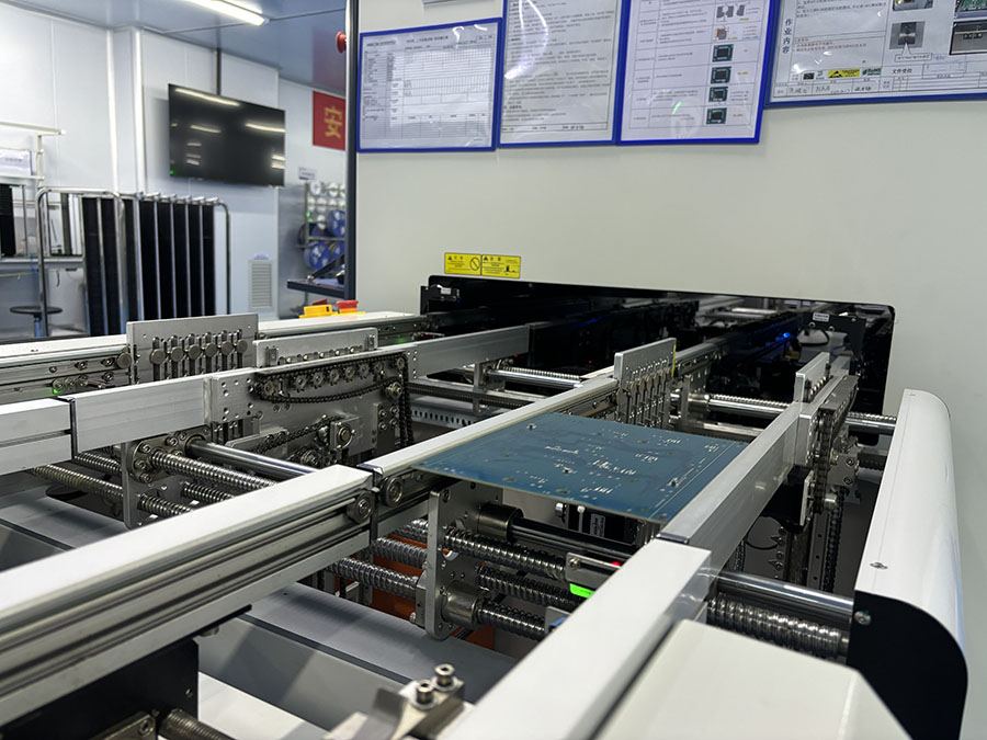
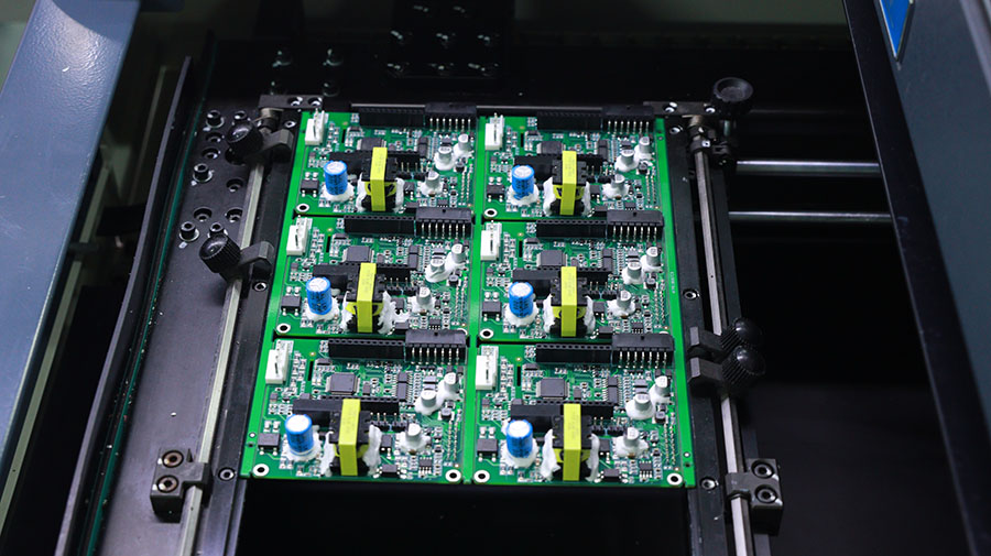
Component placement involves precisely positioning surface-mount devices (SMDs) onto PCB pads. High-speed placement machines equipped with vision systems and multi-nozzle heads achieve speeds exceeding 150,000 placements per hour with ±25 micron accuracy. The placement workflow encompasses solder paste printing, SPI inspection, component pickup, vision alignment, and placement actions. Program optimization requires balancing efficiency and quality.
2.2 Soldering
Soldering establishes electrical and mechanical connections between components and the PCB. Reflow soldering is used for surface-mount components, melting and solidifying solder paste through four temperature zones: preheating, soak, reflow, and cooling, with peak temperatures controlled between 235 and 245 degrees Celsius. Wave soldering targets through-hole components, where molten solder waves contact pins to achieve bonding, requiring flux application and preheating. Selective wave soldering and laser welding address specialized requirements. Soldering quality directly determines connection reliability and long-term stability.
2.3 Testing & Debugging
Testing verifies PCBA functional compliance, while debugging corrects design or process defects. Functional testing (FCT) simulates real-world environments to validate overall system performance. In-circuit testing (ICT) uses probe beds to inspect component parameters and solder quality. Automated optical inspection (AOI) identifies visual defects like missing parts, incorrect components, or solder bridges. X-ray inspection visualizes internal conditions of hidden solder joints like BGAs. Debugging involves root cause analysis of test failures, implementing design optimizations or process adjustments.
3. Quality and Reliability Terminology
3.1 Design for Manufacturability (DFM)
DFM is an engineering methodology integrating manufacturing constraints during product design. Core elements include component selection standardization, package compatibility assessment, process window design, and test accessibility planning. DFM analysis proactively identifies potential manufacturing risks, reduces production costs, and shortens time-to-market.
3.2 Signal Integrity (SI)
Signal integrity focuses on high-speed signal transmission quality, involving critical metrics such as reflection, crosstalk, attenuation, and timing. Control measures include impedance matching design, stackup optimization, termination strategies, and equal-length routing. The goal is to ensure accurate signal transmission at rated speeds, preventing bit errors and system failures.
3.3 Mean Time Between Failures (MTBF)
MTBF is a core metric for product reliability, representing the average operational time between failures. It is calculated through extrapolation from accelerated life test data or field failure statistics. Communication equipment typically requires an MTBF exceeding 100,000 hours, corresponding to an annual failure probability below 0.1%.
4.Conclusion

The PCBA terminology system embodies the technical heritage and process expertise of the electronics manufacturing industry. From substrate preparation to precision assembly, from quality inspection to reliability verification, each term represents the crystallization of engineering practice and theoretical research. Mastering the precise meanings of these terms is a fundamental capability for deeply understanding PCBA technology, facilitating professional collaboration, and driving industry innovation.