
Solder cracks are a significant hidden hazard affecting the reliability of electronic products, and are closely linked to thermal stress, material compatibility, process parameters, structural design and environmental factors. This article analyses the prevalence of the five main causes and their corresponding solutions, helping to improve soldering quality and product reliability.

1.How Thermal Shock Leads to Cracks
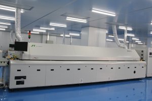
Thermal shock accounts for 38% of solder joint cracks. Improper settings for the reflow soldering temperature profile lead to differences in coefficients of thermal expansion (CTE). In double-sided assembly processes, secondary reflow generates additional thermal shock, whilst mismatched CTEs between large-size BGAs and the PCB substrate cause interfacial stress. These factors cause cumulative damage to solder joints during repeated thermal cycling, ultimately resulting in cracks.
2.How Material Compatibility Affects Soldering
Material compatibility issues account for 25%. Mismatches between solder paste alloy composition and component lead plating—such as the combination of SnAgCu solder paste with OSP-treated pads—can easily lead to interfacial embrittlement. Insufficient temperature resistance in the PCB solder mask material causes delamination, whilst mismatched reactivity between solder and flux affects wetting quality. Uncontrolled reactions at material interfaces are the intrinsic root cause of crack initiation.
3. How Deviations in Process Parameters Cause Cracks
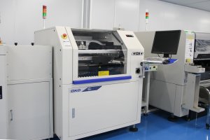
Deviations in process parameters account for 22%. Placement pressure exceeding the component’s tolerance range, particularly for components with bottom pads such as QFNs, is prone to damage. Insufficient nitrogen shielding concentration leads to oxidation and embrittlement of solder joints, whilst excessive cooling rates generate micro-cracks. Loss of control over parameters causes deterioration of the internal structure of solder joints, resulting in reduced load-bearing capacity.
4.How Structural Design Defects Cause Stress Concentration
Structural design defects account for 12%. Mismatches in pad-to-component dimensions exceeding 15%, unreasonable via design leading to stress concentration, and high-density component layouts generating mechanical stress. Inherent structural deficiencies cause solder joints to bear additional loads during service, accelerating crack propagation.
5.How Environmental Factors Accelerate Deterioration
Environmental factors account for 3%. Fluctuations in workshop temperature and humidity exceed standard ranges; ideal values are 23 ± 3 °C and 40–60% RH. Mechanical vibrations during handling exceed permissible limits, whilst storage environments are contaminated by sulphuric gases. The superposition of environmental stresses and thermomechanical stresses shortens the fatigue life of solder joints.
6.How to Optimise Thermal Management Solutions
Establish a database of dynamic temperature curves, matching 12 standard curves to component thicknesses ranging from 0.5 to 6.0 mm. Implement a segmented cooling system to precisely control the cooling rate at 4 to 6 degrees Celsius per second. Apply selective soldering processes to high-density boards to reduce overall thermal shock.
7. How to Strengthen Materials Science Control
Equip facilities with XRF spectrometers for solder composition verification and establish a materials compatibility matrix database covering 256 common material combinations. Develop specialised solder paste formulations to enhance crack resistance, ensuring material interface reliability from the source.
8. How to Build an Intelligent Process Control System
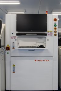
Configure an online SPI inspection system with an accuracy of ±5 micrometres. Deploy 3D AOI (Automated Optical Inspection) with a minimum detection size of 0.01 square millimetres. Implement CPK (Process Capability Index) monitoring with a target value of ≥1.67 to achieve real-time closed-loop control of process parameters.
9.How to Implement Reliability-Enhanced Design
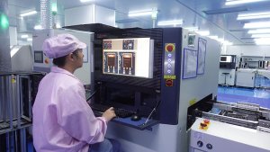
Provide a free Design for Manufacturability (DFM) review service to optimise pad design. Apply underfill processes to critical solder joints to distribute stress. Develop design specifications for stress-relief structures to enhance resistance to deformation.
10.How to Establish a Quality Traceability System
Utilise an MES system to record process parameters for each board, enabling end-to-end data traceability. Employ dual verification through metallographic section analysis combined with SEM scanning electron microscopy inspection, and provide solder joint tensile strength test reports compliant with IPC-9701 standards.
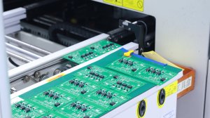
The prevention and control of SMT solder cracks requires a systematic approach across five dimensions: thermal management, materials, processes, design and environment. By accurately identifying the proportion of causes and implementing targeted optimisation measures, the defect rate of cracks can be reduced to an extremely low level, ensuring the long-term reliability of electronic products.
