
The rapid growth of artificial intelligence has created unprecedented demand for specialized computing hardware, from GPU accelerators to edge AI processors. At the heart of this revolution lies AI hardware PCB assembly—the manufacturing process that transforms bare boards and electronic components into functional AI computing platforms. Unlike conventional electronics, AI systems push every physical limit: ultra-high component density, extreme thermal loads, and signal speeds that leave no room for error. As a leading PCB assembly manufacturer, Keep Best PCBA recognizes that building reliable AI hardware requires a fundamentally different approach to PCB assembly.
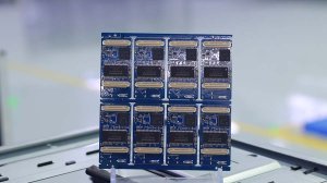
Why AI Hardware Demands a New Approach to PCB Assembly
AI hardware is not simply a faster version of traditional computing equipment. The architectures powering large language models, computer vision systems, and autonomous driving platforms operate at frequencies and power levels that conventional PCB design never anticipated. This makes AI hardware PCB assembly one of the most demanding specialties in modern electronics manufacturing.
Several factors set AI hardware apart from standard PCB assembly projects:
- Extreme power density: AI accelerators consume hundreds of watts in compact footprints, generating heat that must be dissipated through the PCB itself
- Ultra-fine pitch components: Modern AI chips use packaging technologies like FCBGA and chiplets with sub-0.3mm pitch, requiring placement accuracy measured in microns
- Multi-layer complexity: AI hardware PCBs routinely exceed 20 layers, with blind and buried vias creating intricate interconnect patterns
- High-speed signal requirements: Data rates exceeding 56 Gbps between AI chips demand controlled impedance and minimal signal loss
These requirements mean that AI hardware PCB assembly cannot rely on standard SMT lines alone. It requires specialized equipment, rigorous process control, and deep engineering expertise at every stage of production.
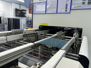
Key Challenges in AI Hardware PCB Assembly
High-Density Interconnect and Component Placement
AI hardware packs more functionality into smaller spaces than any previous electronics category. A typical AI accelerator module may combine a large GPU die, multiple HBM memory stacks, voltage regulators, and high-speed interconnects—all on a substrate measuring less than 100mm per side. This density creates significant challenges for AI hardware PCB assembly teams.
SMT placement machines must handle components ranging from 0201 passives to 75mm FCBGA packages on the same board. The placement accuracy requirement for sub-0.3mm pitch components is typically plus or minus 25 microns or better. Even slight misalignment can cause open circuits or solder bridges that render the entire module useless, making precision placement non-negotiable in AI hardware PCB assembly.
Thermal Management During Assembly
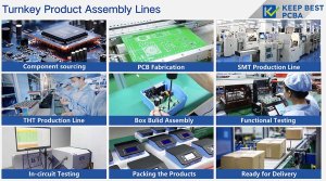
AI chips generate enormous heat during operation, but thermal challenges begin during the assembly process itself. The large thermal mass of copper-heavy AI PCBs means that reflow soldering profiles must be carefully tuned to ensure proper solder joint formation across components of vastly different sizes.
Key thermal considerations in AI hardware PCB assembly include:
- Reflow profile optimization for boards with 20-plus layers and heavy copper planes
- Managing temperature differentials across large BGA components to prevent solder ball cracking
- Selecting solder pastes that perform reliably at elevated operating temperatures
- Integrating thermal interface materials during box build assembly
Signal Integrity and High-Frequency Performance
AI hardware operates at signal speeds that make every PCB design decision critical. At 56 Gbps and beyond, even minor variations in trace geometry, dielectric thickness, or copper surface roughness can cause signal degradation that cripples performance. AI hardware PCB assembly must preserve the signal integrity designed into the board without introducing manufacturing-induced losses.
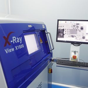
This requires precise control over solder paste volume, component coplanarity, and via plating uniformity. X-ray inspection becomes essential not just for solder joint quality, but for verifying that high-speed via structures are free from voids that could disrupt signal paths in AI hardware PCB assembly.
Advanced Solutions for AI Hardware PCB Assembly
SMT Assembly Optimized for AI Hardware
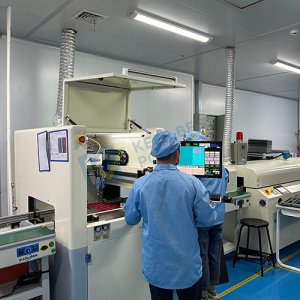
Modern AI hardware PCB assembly relies on SMT equipment specifically configured for high-density, high-mix production. High-speed placement systems with dual-gantry configurations can handle the component variety typical of AI modules while maintaining the placement accuracy that fine-pitch devices demand.
Key SMT capabilities for AI hardware include:
- 3D solder paste inspection (SPI): Validates paste volume and height for every pad before placement, catching deposition errors early
- Multi-camera placement verification: Confirms component alignment and orientation in real time during placement
- Adaptive reflow profiling: Uses thermal profiling data to adjust zone temperatures for optimal solder joint formation
3D AOI and X-Ray Inspection
Inspection technology is where AI hardware PCB assembly truly diverges from standard production. Two-dimensional AOI cannot adequately inspect the hidden solder joints beneath large BGA packages or verify the coplanarity of multi-chip modules. Advanced 3D AOI systems provide the height data needed to detect tombstoning, solder bridging, and insufficient solder on fine-pitch components.
X-ray inspection is equally critical. For AI hardware, X-ray systems must not only detect solder voids but also measure their size and location relative to high-speed signal paths. Keep Best PCBA deploys 3D X-ray inspection as part of its one-stop PCBA solution for AI hardware customers, ensuring that every joint meets the stringent quality standards that AI applications demand.
DFM Analysis Tailored for AI Hardware
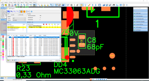
Design for Manufacturability analysis is essential for any PCB assembly project, but AI hardware PCB assembly requires a specialized DFM approach. Standard DFM checks focus on basic manufacturability—trace width, pad size, solder mask clearances. AI hardware DFM must additionally evaluate:
- Thermal via patterns and their impact on solder paste flow during reflow
- Component placement density and its effect on reflow uniformity across the board
- High-speed signal routing and potential manufacturing-induced impedance variations
- Panelization strategy for oversized AI modules with complex routing requirements
By conducting thorough DFM analysis before production begins, manufacturers can identify and resolve potential issues that would otherwise cause costly failures during AI hardware PCB assembly.
Industry Applications: Where AI Hardware PCB Assembly Matters Most
The demand for specialized AI hardware PCB assembly spans multiple industries, each with unique requirements and certification standards:
- Data centers: AI accelerator cards and inference servers require high-reliability assembly capable of continuous operation under extreme thermal loads
- Autonomous vehicles: Edge AI modules for self-driving systems must meet automotive grade standards while delivering maximum computing density in minimal space
- Robotics: AI-powered robots need compact, rugged PCB assemblies that combine inference capability with motor control and sensor interfaces
- Industrial IoT: Smart factory edge devices leverage AI hardware for real-time quality inspection and predictive maintenance applications
- Consumer electronics: AI-enhanced smartphones, wearables, and smart home devices push the boundaries of miniaturization in PCB assembly
Each application brings its own certification requirements. Automotive AI hardware may require IATF 16949 compliance, while medical AI devices need ISO 13485 certification. Choosing a manufacturer with broad certification coverage ensures that AI hardware PCB assembly meets the right standards for each target market.

Best Practices for AI Hardware PCB Assembly Projects
Whether you are developing a prototype AI accelerator or preparing for mass production, several best practices can significantly improve outcomes in AI hardware PCB assembly:
- Involve your manufacturer early: Engage DFM analysis during the design phase, not after. Early feedback on thermal via patterns, component selection, and panelization can prevent costly redesigns
- Specify inspection requirements upfront: Define which joints require X-ray inspection, what void percentage is acceptable, and what AOI criteria apply to fine-pitch components
- Plan for thermal validation: Include thermal test points in the design and specify thermal imaging during prototype validation to catch hotspots before mass production
- Choose the right solder paste: AI hardware often requires no-clean, halogen-free solder pastes with excellent printing performance at fine pitch and reliable reflow characteristics
- Document traceability requirements: AI applications in automotive and medical markets require full component and process traceability—specify these needs before production begins
The Future of AI Hardware PCB Assembly
As AI models grow larger and AI hardware becomes more powerful, the demands on PCB assembly will only intensify. Emerging trends that will shape the future of AI hardware PCB assembly include:
- Chiplet architectures: Multi-die packages will require even finer pitch assembly and more sophisticated inspection methodologies
- Advanced substrates: Glass substrates and silicon interposers will push SMT equipment to new precision limits
- AI-assisted manufacturing: Machine learning algorithms will optimize placement, reflow, and inspection processes in real time
- Sustainable manufacturing: Lead-free PCB assembly processes and energy-efficient production will become standard as environmental regulations tighten globally
Manufacturers that invest in these capabilities today will be best positioned to serve the rapidly growing AI hardware market tomorrow.
Conclusion
AI hardware PCB assembly represents one of the most challenging and rewarding frontiers in electronics manufacturing. The combination of extreme density, thermal intensity, and signal integrity requirements demands specialized equipment, rigorous processes, and deep engineering expertise. From SMT placement and 3D AOI to X-ray inspection and DFM analysis, every step must be optimized for the unique demands of AI hardware.
Keep Best PCBA brings over a decade of experience in electronic manufacturing services, with facilities in Shenzhen, Jiangmen, and Thailand. Our ISO 9001, ISO 13485, and IATF 16949 certifications ensure that your AI hardware PCB assembly project meets the highest quality standards across every industry. Contact Keep Best PCBA to discuss your AI hardware manufacturing needs and discover how our advanced capabilities can bring your AI innovations to market.
