
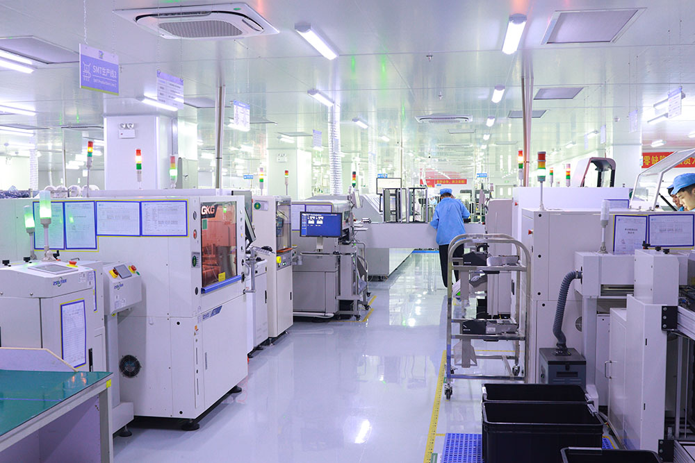
The intersection of artificial intelligence and printed circuit board assembly is no longer a future concept. In 2026, AI hardware PCB assembly represents a fundamental shift in how electronics manufacturers approach quality, throughput, and process control. From machine vision systems that inspect solder joints in real time to MES platforms that track every component from reel to finished board, the smart factory has moved from pilot projects to production floors across China and Southeast Asia.
For companies building artificial intelligence hardware, edge computing devices, and high-performance computing platforms, the demands on PCB assembly have grown more stringent than ever. Boards now carry denser component packages, higher layer counts, and tighter impedance tolerances. Traditional inspection and process control methods, designed for an earlier era of electronics manufacturing, cannot keep pace. This guide examines the specific smart factory technologies that are reshaping PCB assembly manufacturer operations and explains how these innovations translate into measurable improvements in yield, cost, and time-to-market.
What Is AI Hardware PCB Assembly?
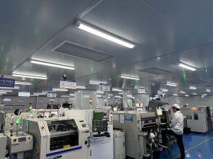
AI hardware PCB assembly refers to the integration of artificial intelligence, machine learning, and advanced automation technologies into every stage of the PCB manufacturing process. It encompasses AI-powered inspection systems, predictive maintenance algorithms, real-time process optimization, and digital twin simulations that model the entire production line before a single board is built.
The term also covers the assembly of PCBs designed specifically for AI applications. These boards typically carry high-pin-count BGAs, dense FPGA clusters, HBM memory stacks, and specialized accelerators that demand tighter process windows and more rigorous quality verification than standard consumer electronics. The convergence of AI as a manufacturing tool and AI as the product being manufactured creates a compounding effect: smarter factories build smarter hardware, which in turn drives further factory innovation.
Key Smart Factory Technologies Transforming PCBA
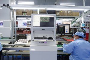
Several discrete technologies form the backbone of the modern smart factory in PCB assembly. Each addresses a specific bottleneck in the traditional manufacturing flow, and together they create a connected, data-driven production environment.
3D Automated Optical Inspection (3D AOI)
Traditional 2D AOI systems capture top-down images of solder joints and component placement, flagging defects based on contrast and pattern matching. 3D AOI goes further by constructing a height map of every solder joint on the board. This added dimension allows the system to detect coplanarity issues on BGA packages, insufficient solder volume, and lifted leads that 2D inspection simply cannot see.
Modern 3D AOI machines use structured light projection and multi-angle cameras to capture solder joint geometry in under one second per board. Machine learning models trained on millions of joint images classify each joint as pass, marginal, or fail with a false-call rate below 50 ppm. For AI hardware PCB assembly, where BGA voiding and head-in-pillow defects can cause catastrophic field failures in high-performance computing systems, 3D AOI is now considered essential rather than optional.
MES Traceability and Digital Thread
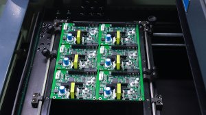
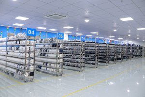
Manufacturing Execution Systems (MES) create a digital thread that connects every process step from incoming material inspection to final test. Each board carries a unique serial number, and every operation performed on it, including solder paste print data, pick-and-place coordinates, reflow profile, AOI results, and ICT/FCT measurements, is logged against that serial number.
This level of traceability serves two critical purposes. First, it enables root-cause analysis when a defect is found downstream. If X-ray inspection flags a BGA void on board number 4,271, the MES system can retrieve the exact reflow profile, paste batch, and stencil cycle count for that specific board, pinpointing the process deviation that caused the defect. Second, it supports compliance requirements for automotive (IATF 16949), medical (ISO 13485), and aerospace applications where component-level traceability is mandatory.
Predictive Maintenance with Machine Learning
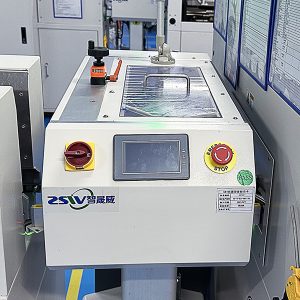
Equipment failure is one of the most disruptive events on a PCB assembly line. A sudden reflow oven heater failure can scrap an entire batch of boards before operators notice the temperature drop. Predictive maintenance uses sensor data from production equipment, including heater currents, conveyor motor vibration, vacuum pump pressure, and stencil cleaner cycle counts, to predict failures before they occur.
Machine learning models analyze patterns in this sensor data to identify early warning signs that precede failures. A slight increase in vacuum pump current over two weeks, for example, may indicate an impending pump failure. The system alerts maintenance staff to schedule replacement during a planned downtime window, preventing unplanned line stoppages. For high-volume AI hardware PCB assembly lines running 24-hour schedules, predictive maintenance can reduce unplanned downtime by 30 to 50 percent.
How Does Digital Twin Technology Optimize PCBA Lines?
A digital twin is a virtual replica of the physical production line. It models every machine, conveyor, process parameter, and material flow in software, allowing engineers to simulate process changes, test new product introductions, and optimize line balancing without disrupting actual production.
When a new AI accelerator board is ready for production, the digital twin simulation runs the complete assembly sequence virtually. It predicts solder paste deposition patterns, identifies potential placement collisions, estimates cycle time, and flags thermal management concerns on high-density BGA clusters. Engineers use these simulation results to refine the process recipe and line configuration before the first physical board is built. This approach reduces NPI cycle time by 40 to 60 percent compared to traditional trial-and-error line setup.
Digital twins also support continuous optimization. Real production data from the MES system feeds back into the twin, keeping the virtual model synchronized with physical reality. When the twin detects a gradual drift in placement accuracy or reflow temperature uniformity, it recommends parameter adjustments that keep the line within its optimal operating window.
AI-Powered Solder Paste Inspection and Process Control
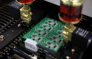
Solder paste printing accounts for approximately 60 percent of all SMT defects. Even small variations in paste volume, deposition shape, or alignment can lead to insufficient solder, bridging, or tombstoning downstream. AI-powered solder paste inspection (SPI) systems address this bottleneck with machine learning models that analyze every printed pad on every board.
- Volumetric measurement: 3D SPI systems measure paste height, area, and volume on every pad. AI models compare these measurements against the golden paste volume for each pad type and flag deviations that correlate with downstream defects.
- Pattern recognition: Machine learning models identify systematic patterns in paste deposition errors, such as stencil clogging trends or squeegee wear, and alert operators before defect rates increase.
- Closed-loop correction: Advanced SPI systems connect directly to the paste printer, automatically adjusting squeegee pressure, speed, and stencil cleaning frequency based on real-time measurement data. This closed-loop feedback can reduce paste-related defects by over 70 percent.
- Stencil life prediction: AI models track paste transfer efficiency across thousands of print cycles and predict when a stencil needs cleaning or replacement, preventing the gradual quality degradation that traditional fixed-interval cleaning schedules miss.
For AI hardware PCB assembly, where fine-pitch components and 0201 or 01005 chip placements are common, the precision of solder paste deposition directly determines first-pass yield. AI-powered SPI has moved from an optional enhancement to a core process control requirement.
X-Ray Inspection and AI Defect Classification
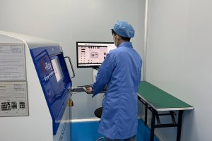
X-ray inspection has long been essential for verifying BGA joint integrity, through-hole solder fill, and QFN thermal pad coverage. The latest generation of X-ray systems pairs high-resolution imaging with AI-powered defect classification, dramatically improving both inspection speed and accuracy.
Traditional X-ray inspection relies on trained operators to manually review images and identify voiding, insufficient solder, or bridging under components. This process is slow and subject to operator variability. AI classification models, trained on annotated X-ray libraries containing hundreds of thousands of joint images, can automatically classify defects with accuracy rates exceeding 98 percent and process times of under five seconds per board.
For AI hardware applications that use complex package configurations such as multi-die modules, package-on-package stacks, and embedded components, automated X-ray classification provides the inspection depth that manual review cannot achieve at production scale. The combination of 3D AOI for surface-level defects and AI-augmented X-ray for hidden joint defects creates a comprehensive inspection net that catches virtually every assembly defect before boards leave the factory.
What Role Does IoT Play in Smart Factory PCBA?
Internet of Things sensors embedded throughout the production line create a continuous data stream that feeds AI models and MES dashboards. Temperature and humidity sensors in the SMT area monitor the production environment, ensuring it stays within the narrow window that solder paste manufacturers specify. RFID readers on material storage cabinets track component shelf life and enforce first-in-first-out usage to prevent expired materials from reaching the line.
Connected pick-and-place machines report vacuum nozzle performance data in real time, allowing AI models to predict nozzle wear and schedule replacement before placement accuracy degrades. Smart feeders log component pickup success rates and alert operators when a specific feeder slot begins underperforming, preventing the cascading placement errors that a single faulty feeder can cause across an entire production run.
The IoT infrastructure also supports energy management and sustainability initiatives. Smart meters on reflow ovens, wave soldering systems, and burn-in chambers identify energy waste and enable scheduling optimizations that reduce peak demand charges. For a one-stop PCBA solution provider operating multiple SMT lines, these energy savings compound across thousands of production hours per year.
Industry 4.0 and the Future of Electronics Manufacturing
The technologies described above, AI inspection, MES traceability, predictive maintenance, digital twins, and IoT connectivity, collectively define what Industry 4.0 means for PCB assembly. The vision extends beyond individual smart machines to a fully connected, self-optimizing production ecosystem.
Cyber-Physical Production Systems
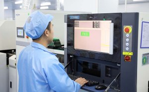
In a true Industry 4.0 factory, every machine, sensor, and software system communicates through standardized protocols. When a 3D AOI system detects a trend in solder volume deviation, it does not just flag the defect. It communicates directly with the paste printer to adjust squeegee parameters, notifies the MES system to tag affected boards for enhanced downstream inspection, and logs the event in the predictive maintenance model that monitors stencil health. This autonomous feedback loop is the essence of a cyber-physical production system.
Cloud-Based Process Analytics
Cloud platforms aggregate production data across multiple factory sites, enabling cross-site benchmarking and best-practice transfer. When a process engineer at the Shenzhen facility discovers a reflow profile optimization that reduces BGA voiding by 15 percent, the cloud analytics platform can identify similar product configurations at the Thailand factory and recommend the same profile adjustment there. This capability turns isolated improvements into systemic gains across the entire manufacturing network.

Human-AI Collaboration
The smart factory does not eliminate human expertise. It augments it. AI systems handle repetitive inspection tasks, anomaly detection, and process optimization at speeds and scales that exceed human capability. Engineers and operators focus on complex problem-solving, new product introduction, and process engineering decisions that require contextual judgment. The most successful AI hardware PCB assembly operations pair skilled engineering teams with AI tools, creating a collaborative environment where each compensates for the other’s limitations.
How to Evaluate a Smart Factory PCBA Partner
Selecting a manufacturing partner that has genuinely adopted smart factory technologies requires looking beyond marketing claims. Several concrete indicators distinguish a true Industry 4.0 operation from a traditional factory with a digital dashboard.
- Inspection capability depth: Does the supplier operate 3D AOI and AI-powered X-ray systems as standard equipment on all lines, not just on a showcase line? Ask for AOI escape rate data and X-ray classification accuracy metrics.
- MES implementation scope: Request a demonstration of the MES traceability system. A genuine MES implementation allows you to look up any serial number and see the complete process history, including paste print data, placement coordinates, reflow profile, and test results.
- Data accessibility: Can the supplier share production data, SPC charts, and yield reports in real time through a customer portal or API? Data transparency is a hallmark of mature smart factory operations.
- Predictive maintenance maturity: Ask about equipment maintenance strategy. If the answer is preventive maintenance on fixed schedules, the factory has not yet adopted predictive approaches.
- Digital twin usage: For new product introductions, does the supplier use simulation tools to validate the process recipe before production? This capability significantly reduces NPI risk and time.
- Continuous improvement evidence: Look for documented yield improvement trends over time. Smart factory technologies should produce measurable, sustained quality gains, not just impressive dashboards.
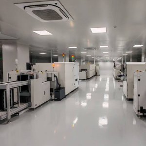
AI hardware applications demand manufacturing partners who have invested in the technologies that match the complexity of the products being built. A factory still relying on 2D AOI, manual X-ray review, and paper-based traceability cannot meet the quality and consistency requirements of modern AI accelerator boards and edge computing modules.
The Competitive Edge of Smart Factory PCBA in 2026
The factories that have embraced AI-driven manufacturing are pulling ahead of those that have not. The data tells the story clearly. First-pass yield improvements of 3 to 8 percentage points, defect escape rates below 200 ppm, NPI cycle time reductions of 40 percent or more, and unplanned downtime reductions of 30 to 50 percent are typical outcomes for mature Industry 4.0 implementations.
For companies developing AI hardware, these improvements translate directly into faster time-to-market, lower field failure rates, and the ability to scale production volumes without proportionally scaling inspection labor. As the AI hardware market continues its rapid growth, the manufacturing partners who can support that growth with smart, data-driven, AI-augmented production capabilities will define the competitive landscape.
Contact Keep Best PCBA for professional AI hardware PCB assembly services backed by 3D AOI, AI-powered X-ray inspection, full MES traceability, and smart factory capabilities across our Shenzhen, Jiangmen, and Thailand facilities.
