

Every redesign cycle costs engineering hours, prototyping budget, and launch momentum. A board that fails its first prototype run wastes ten days of NPI time and triggers cascading purchasing, certification, and customer commitments. DFM analysis for PCB assembly exists to prevent exactly this scenario by checking the design against manufacturing reality before a single panel is fabricated. When applied systematically, DFM review turns first-pass yield from a coin-flip into a predictable outcome that experienced PCB assembly manufacturer operations achieve on every production batch.
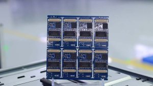
This guide walks through seven practical PCB design for manufacturing rules that consistently lower assembly cost, reduce solder defects, and shorten lead times. The focus is real-world rules your CM can verify with their processes and equipment, not theoretical guidelines that exist only in textbooks. The same rules apply whether you ship a five-piece IoT prototype or a fifty-thiece-unit automotive controller program, and they form the foundation of any reliable one-stop PCBA solution from prototype to mass production.
What Is DFM Analysis in PCB Assembly?
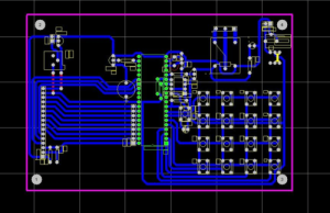
Design for Manufacturing (DFM) is the practice of reviewing a PCB layout against the constraints, tolerances, and capabilities of the assembly process before fabrication. DFM analysis identifies issues that would otherwise surface only after the first prototype run: trace-to-pad misalignment, missing solder mask slivers, fiducial placement errors, panelization inefficiencies, component orientation problems, and silkscreen collisions with pads. Catching these issues in the CAD stage costs cents. Catching them on the assembly line costs dollars per unit, plus schedule slippage.
Professional PCBA operations run a structured DFM check at three points in the product lifecycle. The first check happens before Gerber release, when the design is still fluid. The second happens at NPI kickoff, when the fabricator and assembler review stackup, panel layout, and BOM risk. The third happens on the first article, when AOI, X-ray, and ICT data are used to refine the design for the next revision. Each check has a different goal and a different cost-to-fix ratio.
Why DFM Matters More in 2026
Three trends have made DFM more important than ever. First, component miniaturization has pushed most packages below 0402 imperial size, where solder joint inspection requires X-ray rather than optical AOI. Second, lead-free assembly profiles run 30 to 40 degrees hotter than legacy tin-lead, narrowing the process window for heat-sensitive components. Third, supply chain volatility has pushed engineers toward second-source and alternate-part substitutions, which often introduce new footprint, thermal, and paste-deposit considerations that the original design never accounted for. A disciplined DFM workflow addresses all three trends in parallel.
DFM Rule 1: Optimize Component Placement for Pick-and-Place Efficiency
Component placement is the single biggest driver of assembly throughput and first-pass yield. Group similar packages together so the pick-and-place machine can use a single feeder bank without interrupting motion for nozzle changes. Keep all polarized components in the same orientation, ideally with pin one indicators aligned in one direction across the entire board. Place tall components on one side and short components on the other side when running a mixed-technology two-sided reflow board to avoid shadowing during the second pass.
Maintain a 0.5 mm clearance between components and board edges, and a 1.0 mm clearance between discrete components and the edge of any BGA or QFN. Components placed too close to the board edge risk being damaged during depanelization. Components placed too close to fine-pitch packages disturb the local paste deposit during placement and create solder bridges.

Component-to-Component Spacing Recommendations
- 0402 to 0402: minimum 0.2 mm edge-to-edge, 0.3 mm preferred for hand-rework clearance.
- SOIC to nearby discrete: minimum 0.5 mm, 0.8 mm preferred to avoid tombstoning during reflow.
- BGA to nearby passive: minimum 1.0 mm to prevent placement nozzle collision.
- Tall heatsink to nearby component: maintain 2.0 mm clearance so the heatsink does not trap heat during reflow and cause cold joints.
DFM Rule 2: Follow Trace and Spacing Rules That Match Your Fab Capability
Trace width and spacing must match the PCB fabricator’s manufacturing capability, not just the electrical requirement. Most volume fabricators produce 4 mil trace and space as standard, with 3 mil available at premium. Going below 3 mil pushes yield below 95 percent on most processes and dramatically raises cost. Going above 6 mil produces no electrical benefit but allows the fabricator to use lower-cost processes and improves etch uniformity.
Maintain consistent trace width within a single net where possible. Sharp 90-degree bends should be avoided at frequencies above 100 MHz, but for digital logic below 50 MHz, the bend angle is irrelevant compared to the etching tolerance. Use teardrops where traces enter pads or vias, especially on fine-pitch QFN and BGA layouts. Teardrops reduce drill breakout failures by 40 to 60 percent on most processes.

Via and Pad Geometry Considerations
- Via diameter: 0.3 mm mechanical drill with 0.6 mm pad is the volume sweet spot for most 4-layer designs.
- Via-in-pad: acceptable for BGA breakouts but requires filling and planarizing, which adds 8 to 12 percent to PCB cost.
- Annular ring: maintain at least 0.15 mm beyond the drilled hole for fab tolerance.
- Mask slivers: avoid solder mask slivers narrower than 0.1 mm between adjacent pads, which dissolve during reflow and create solder bridges.
DFM Rule 3: Plan Stackup Early With the Fabricator, Not After the Layout Is Finished
Stackup decisions lock in impedance control, layer count, and material cost long before the first trace is routed. A 4-layer stackup with 0.2 mm core, 0.36 mm prepreg, and 1 oz copper is the volume workhorse for most consumer and industrial designs above 50 MHz. For designs above 500 MHz, 6-layer stackup with dedicated ground and power planes is required to control impedance and reduce EMI. For high-current power designs, 2 oz copper on inner layers is the standard.
The most expensive stackup decision a team can make late is adding a layer after the layout is complete. Adding one layer mid-design typically costs three engineering weeks of re-routing plus one to two weeks of new prototyping, because all through-hole vias and BGA breakouts must be reworked. Decide stackup before routing the first net.
DFM Rule 4: Add Fiducials and Panelization Features for Automated Assembly
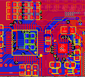
Fiducials are the reference markers that allow the pick-and-place machine, AOI, and screen printer to align to the board. Every assembly panel needs at least three fiducials: two on opposite corners for global alignment and one near any fine-pitch component for local alignment. Panel fiducials should be 1.0 mm bare copper with 3.0 mm mask opening. Local fiducials near QFN, BGA, or 0201 packages should be 0.5 mm bare copper with 1.5 mm mask opening.
Panelization determines how efficiently the fabricator can produce boards and how cleanly the assembler can depanelize them. V-cut panels are cheapest but require a 12 mm keep-out from the board outline for the cutting wheel. Tab-routed panels with mouse-bite connections allow tighter board packing but require a de-tabbing step that adds labor cost. For prototypes below ten units, tab routing is faster. For volume production, V-cut is more economical.
Common Fiducial Mistakes to Avoid
- Fiducial covered by silkscreen: silkscreen on top of a fiducial prevents accurate camera recognition.
- Fiducial too close to tall component: keep at least 5 mm clearance so the placement camera has clear line of sight.
- Fiducial on breakaway tab: once the tab is removed, the fiducial is gone, so do not place it on a tab that will be separated before final assembly.
- Missing local fiducial: any fine-pitch component below 0.5 mm pitch should have its own local fiducial for sub-pixel alignment.
DFM Rule 5: Match Solder Paste and Stencil Design to Component Density
Solder paste selection and stencil aperture design drive the majority of reflow defects. For standard 0402 and 0603 components, a 0.1 mm stencil with 1:1 aperture ratio is standard. For fine-pitch QFN below 0.5 mm pitch, a 0.12 mm stencil with reduced aperture area (typically 80 percent of the pad) prevents solder bridging. For BGA below 0.8 mm pitch, a 0.1 mm stencil with nanocoating or electroformed foil produces more consistent paste release.
Aperture shape matters as much as size. Round apertures release paste more cleanly than square ones for chips. Home-plate apertures on QFN thermal pads reduce voiding compared to a single large aperture by splitting the thermal pad into multiple paste-release points. Aperture wall finish should be polished, not rough, to reduce paste sticking during release.
DFM Rule 6: Build the BOM for Supply Chain Resilience
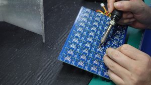
A design that uses only one source for every critical component is fragile. Identify the two to three longest-lead items in the BOM and qualify second sources for each at design time, not during a supply crisis. Common second-source candidates are common logic gates, op-amps, MOSFETs, and passives in standard EIA sizes. For unique parts such as FPGAs, ASICs, and proprietary sensors, plan a minimum 12-week inventory buffer.
Component selection also drives DFM cost. Choosing 0402 over 0201 components doubles placement yield on most processes. Choosing a 0.8 mm pitch QFN over a 0.5 mm pitch QFN reduces stencil and paste-print defects by 60 percent. Choosing an SOIC over a QFN cuts inspection cost by 30 percent because leads are easier to AOI than pads.
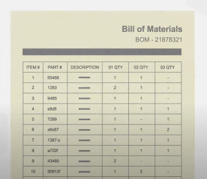
BOM Risk Categories Worth Flagging in DFM Review
- End-of-life components: parts with last-time-buy notices should be replaced before NPI unless an inventory commitment is in place.
- Single-source parts: any part with no qualified second source should be reviewed for redesign to an alternate.
- Long lead time: any part over 16 weeks lead time should be reviewed for inventory strategy.
- Out-of-stock only: any part currently on allocation should be reviewed for immediate substitution.
DFM Rule 7: Document the Assembly Process and Inspection Criteria Up Front
Documentation that lives only in the designer’s head becomes a liability the moment the designer moves to another project. Every NPI release should ship with an assembly process document that specifies the solder paste, stencil, reflow profile, AOI inspection criteria, and any hand-rework instructions. Inspection criteria should be defined per component family: BGA requires X-ray void limits, QFN requires AOI plus X-ray, and through-hole requires wave-solder or selective-solder settings.
IPC-A-610 is the industry standard for acceptance criteria, but the level matters. Class 1 is general consumer electronics, Class 2 is industrial and commercial, and Class 3 is medical, aerospace, and military. Specifying Class 2 where Class 1 is sufficient adds cost without adding value. Specifying Class 3 where Class 2 is required invites field failures. The right IPC class should be defined during the DFM review, not after the first defect appears.

Putting DFM Rules Into a Repeatable Workflow
The seven rules above become valuable only when they are applied consistently across every project. A repeatable DFM workflow has three checkpoints: a CAD-stage review before Gerber release, an NPI-stage review before the first prototype, and a production-stage review after the first 100 units are assembled. Each review uses the same checklist, but the depth of review changes with the program maturity. The first review catches 70 percent of issues. The second review catches 25 percent more. The third review catches the residual process issues that only appear under production volume.
For teams that lack in-house DFM expertise, partnering with an experienced PCBA manufacturer adds a review layer that internal teams cannot match. The right partner runs DFM checks on every new design as a standard service, has the equipment and inspection data to back up their feedback, and can quote DFM-driven cost savings in concrete numbers rather than general guidance. Contact Keep Best PCBA for professional DFM analysis for PCB assembly and a quote on your next design, and let an experienced team review your layout before fabrication starts.
