
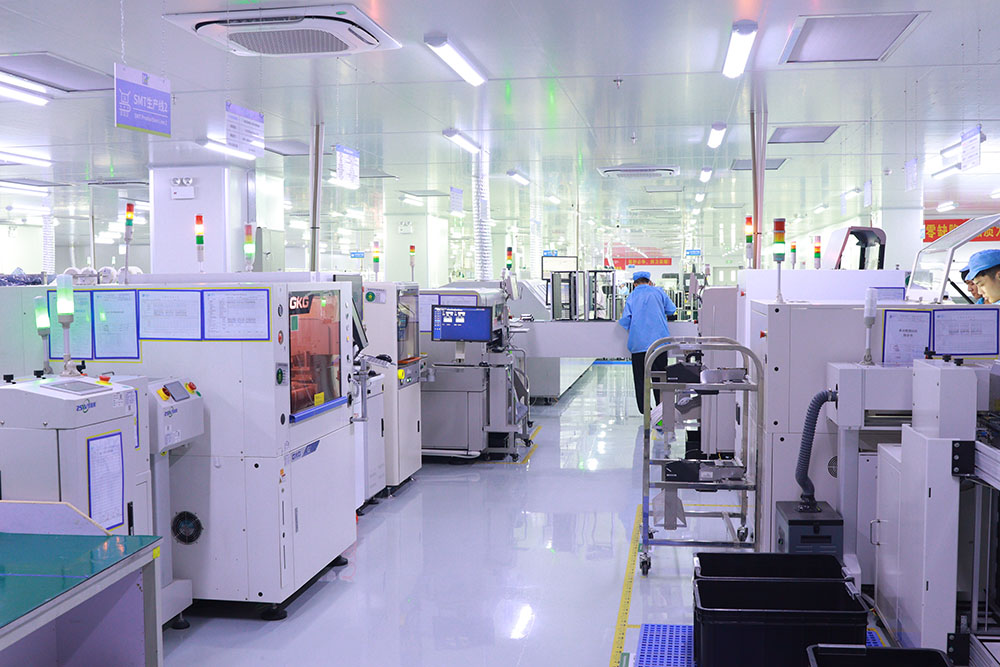
Surface mount dominates modern electronics, but through-hole components remain indispensable for connectors, transformers, large capacitors, and high-power parts that need mechanical strength. Making those joints reliably is the job of wave and selective soldering. Selective soldering vs wave soldering is a decision that affects quality, cost, and flexibility across the product lifecycle, and it deserves deliberate analysis rather than habit or the convenience of existing equipment.
Both processes melt solder and form joints by contacting the board with molten alloy, but they differ sharply in how precisely that contact is applied. Understanding the trade-offs prevents overpaying for capability you do not need, or under-investing in the control a difficult design demands and paying for it later in defects.
How Wave Soldering Works
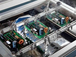
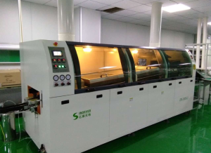
In wave soldering, the entire underside of a board passes over a standing wave of molten solder. Every exposed through-hole lead and pad that touches the wave is soldered in a single pass. It is fast and economical for boards that are predominantly through-hole, and it scales beautifully to very high volumes with minimal labor per board.
Modern wave machines often use nitrogen atmospheres to reduce dross formation and improve wetting, and dual-wave designs handle both broad and fine features in one transit. For high-volume power supplies, relays, and simple controllers, nothing beats its throughput per hour of labor, which is why it remains the workhorse of through-hole production.
How Selective Soldering Works
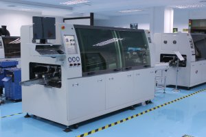
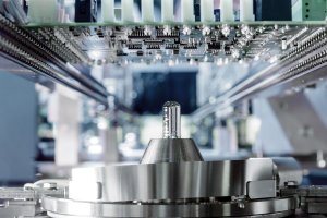
Selective soldering uses a small, programmable nozzle to apply solder only where needed. The board is held still while the nozzle moves underneath, depositing precise amounts of solder at each joint according to a programmed path. Components on the top side are untouched, eliminating the risk of dislodging or heat-damaging them during the pass.
This precision makes selective soldering ideal for mixed-technology boards where surface-mount parts occupy the bottom side alongside through-hole connectors. It also suits low-volume and high-mix production where retooling a wave line for each variant would be impractical or uneconomical, and where flexibility matters more than peak throughput.
Quality and Control
Because solder is localized, selective processes produce consistent joints with minimal bridging and excellent repeatability. Preheat, dwell, and solder volume are tuned per joint type, reducing defects that wave soldering would introduce on crowded boards. A process-savvy
PCB assembly manufacturer programs nozzle path, dwell, and preheat for each joint type, and monitors the process with solder-level and nitrogen-purity controls to keep results stable across long runs.
When Wave Soldering Wins
If your board is mostly through-hole with few top-side parts, wave soldering delivers unmatched speed and lowest cost per joint. High-volume power supplies and simple controllers are classic fits. The trade-off is flexibility: a board design change may require new pallets, new wave parameters, and revalidation of the solder process, which slows response to engineering changes.
When Selective Soldering Wins
Mixed-technology designs, fragile top-side components, and low-to-medium volumes favor selective soldering. Its programmability means a new product needs only a new program, not new tooling, and the selective head reaches joints that wave solder would short or bridge. The slower throughput is the price for that adaptability and for the higher first-pass quality it delivers.
Cost Comparison in Practice
The economic choice depends on volume and mix. At tens of thousands of identical boards, wave soldering amortizes setup across units and wins on cost. At hundreds of variants or lower quantities, selective soldering avoids recurring tooling and changeover expense that would dwarf the per-joint savings of wave. A simple spreadsheet comparing setup, cycle time, and defect cost per unit clarifies the crossover point for a given product.
Defect cost matters as much as cycle cost. If wave soldering on a crowded board produces bridging that requires touch-up, the labor can erase its throughput advantage. Factoring rework into the comparison often flips the recommendation toward selective soldering even at moderate volumes.
Making the Decision
Start with the board architecture. Predominantly through-hole and high volume points to wave; mixed technology and variable volume points to selective. Many shops run both, routing each design to the process that fits its geometry and quantity, and maintaining the flexibility to shift as the product mix evolves with the market.
A pragmatic one-stop PCBA solution helps you weigh throughput against defect risk for each product, so you invest in the right machine time rather than the most expensive option by default. The right answer is frequently different for different products made by the same company, and a good partner will say so.
Hybrid Reality
The cleanest answer is rarely one or the other. Modern lines often reflow the surface-mount side first, then selective-solder the through-hole joints, reserving wave soldering for the rare all-through-hole run. Matching process to product is what keeps both quality and margins healthy, and it lets a single factory serve a broad customer base without forcing every design into one mold.
Understanding both technologies, and the boundary where each excels, is a core competency for any operation that assembles anything more complex than a single-technology board. The savings from choosing correctly accumulate on every unit shipped and compound into a durable cost advantage.
