
PCBs (Printed Circuit Boards) and PCB assemblies are core components in electronics manufacturing, yet they differ fundamentally in functional positioning, manufacturing processes, and application scenarios. This article provides an in-depth analysis of the distinctions and connections between PCBs and PCB assemblies across three dimensions: defining functions, manufacturing processes, and characteristic applications. It aims to help readers systematically grasp the fundamentals of electronics manufacturing.
1.Definition and Functional Comparison
1.1 Basic Definition of PCB
PCB, short for Printed Circuit Board, serves as the physical substrate for electrical connections between electronic components. Conductive circuit patterns are formed on an insulating base material through processes like etching, drilling, and copper plating. It primarily fulfills two core functions: providing mechanical support structures for electronic components and enabling electrical interconnections between them. The PCB itself does not contain active components (e.g., chips, transistors) or passive components (e.g., resistors, capacitors), existing solely as a foundational framework that provides a stable connection environment for subsequent component installation.
1.2 Functional Enhancement of PCB Assembly
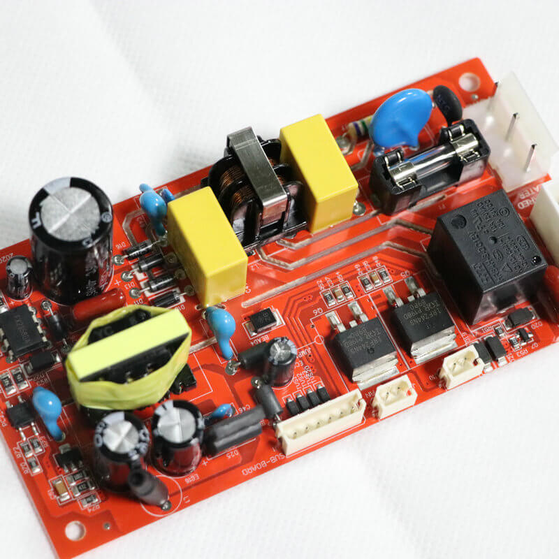
PCB assembly, fully known as Printed Circuit Board Assembly, represents the complete functional form of a PCB. Through SMT (Surface Mount Technology) or THT (Through-Hole Technology) processes, various electronic components are soldered onto the PCB substrate to form assemblies with specific circuit functions. PCBA not only incorporates the PCB substrate but also integrates all necessary electronic components. These components work together to achieve the predefined circuit functionality. As the core component of electronic products, PCBA directly determines the product’s performance metrics, functional realization, and reliability level.
Summary of Core Differences: PCB is the “Skeleton,” providing the foundational connections; PCBA is the “organs,” enabling complete functionality.
2.Manufacturing Process Flow

2.1 Key PCB Manufacturing Processes
Design Phase: Complete PCB layout design based on circuit schematics, determining critical parameters such as layer count, stackup structure, and impedance control.
Substrate Preparation: Select raw materials including copper foil, glass fiber cloth, and epoxy resin to produce laminated copper-clad boards via hot pressing.
Pattern Transfer: Employ photolithography to transfer circuit patterns onto copper foil surfaces, forming precise circuit traces.
Etching: Remove excess copper layers via chemical or laser etching, preserving the required conductive pathways.
Drilling: Create through-holes, blind vias, and buried vias through mechanical or laser drilling for interlayer connections or component mounting.
Metallization: Combining electroless copper plating and electrolytic copper plating creates uniform copper layers on hole walls and circuit surfaces, ensuring conductivity and solderability.
Surface Treatment: Processes like hot air solder leveling (HASL), gold plating, or OSP treat pad surfaces to enhance oxidation resistance and soldering reliability.
Final Inspection: Multi-dimensional quality verification through AOI optical inspection, flying probe testing, impedance testing, etc., ensures finished products meet design specifications.
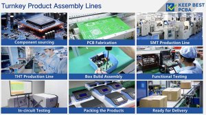
2.2 Core PCB Assembly Processes
Material Preparation: Complete preparation of PCB blanks, electronic components (BOM list), solder paste, stencils, and other production materials.
Solder Paste Printing: Precise application of solder paste onto PCB pads via stencils, with thickness controlled between 80 and 150 microns.
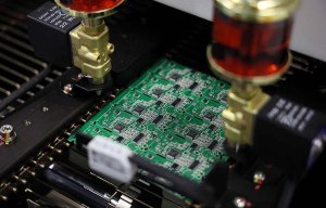
SMT Placement: High-speed placement machines precisely position surface-mount components onto solder paste according to programmed coordinates, achieving ±25 micron accuracy.
Reflow Soldering: Nitrogen-protected reflow ovens melt solder paste along preset temperature profiles to form reliable solder joints.
THT Insertion: Manual or automated insertion of through-hole components such as large connectors and electrolytic capacitors.
Wave Soldering: Through-hole component leads are fixed via wave soldering or selective wave soldering.
Cleaning Process: Removes flux residues and ionic contaminants to meet cleanliness standards.
Functional Testing: Verifies circuit functionality and reliability through ICT inline testing, FCT functional testing, and aging tests.
Packaging and Shipping: Stored in anti-static packaging, ready for final assembly.
3. Characteristics and Application Scenarios
3.1 Core PCB Characteristics
Highly Customizable: Flexible design based on circuit complexity—number of layers (single-sided to multi-layer boards), substrate types (FR-4, high-frequency boards, metal core boards, etc.), and specialized processes (impedance control, blind/buried vias, rigid-flex combinations).
Manufacturing Standardization: Adherence to IPC-6012, IPC-A-600 to ensure consistent product quality and global supply chain compatibility.
Design Flexibility: Supports diverse design requirements from simple single-sided boards to complex high-density interconnect (HDI) boards, catering to applications across consumer electronics, communication equipment, industrial control, and other fields.
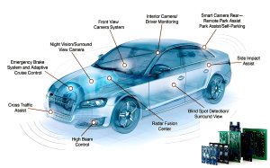
Wide Applicability: As a foundational material in the electronics industry, PCBs are used in nearly all electronic product sectors including smartphones, computers, home appliances, automotive electronics, medical devices, and aerospace.
3.2 Core Characteristics of PCB Assembly
Functional Integrity: Integrates all circuit functions, enabling direct installation into end-devices for system-level debugging. Serves as the “plug-and-play” core module for electronic products.
System Integrity: Comprises the PCB substrate, all components, and soldered interconnections to form a complete electronic functional unit capable of operation without additional components.
High Reliability: Undergoes comprehensive quality control including incoming material inspection, process control, functional testing, and aging screening, achieving MTBF exceeding tens of thousands of hours.
Application Specificity: Directly targets end-product manufacturing, customized to OEM specifications, and participates in final assembly, testing, and certification processes.
4.Relationship and Industrial Value
4.1 Industrial Chain Synergy
PCB and PCBA constitute upstream and downstream segments of the electronics manufacturing industrial chain. PCB manufacturing belongs to the basic material processing segment, with technical barriers concentrated in precision pattern transfer and interlayer interconnection processes. PCBA assembly belongs to the electronic equipment manufacturing segment, with core technologies in precision placement, soldering process control, and inspection techniques. The two complement each other: PCBs provide the physical carrier for PCBA, while PCBA endows PCBs with functional value, jointly driving the evolution of electronic products toward miniaturization, high performance, and high reliability.
4.2 Technological Development Trends
PCB Technology Direction: Higher layer counts (>50 layers), finer line widths (<30 microns), higher-frequency materials (low Dk/Df laminates), and more advanced packaging substrates (IC substrates, substrate-like SLP).
PCB Assembly Technology Directions:
Smaller components (01005/008004 packages), higher density (SiP system-level packaging), smarter production (Industry 4.0 digital factories), greener processes (lead-free, low-energy consumption).
5.Conclusion
Though PCB and PCB assembly share similar names, they fundamentally represent distinct stages in electronics manufacturing. Understanding their definitional differences, process characteristics, and functional roles is key to grasping the fundamentals of the electronics manufacturing industry. Driven by the wave of intelligent and digital transformation, PCB and PCBA technologies continue to converge and innovate, providing robust hardware support for strategic emerging industries such as 5G communications, artificial intelligence, and new energy vehicles.