
Wave soldering is the mainstream process for soldering through-hole components (THT) and is also used for secondary soldering on some mixed-assembly boards. This article analyzes the principles, parameter control, and common defects of wave soldering.
Basic Principles of Wave Soldering
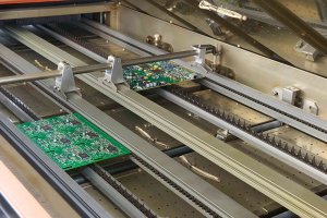
Molten solder forms a wave, and the PCB passes through it at a specific angle and speed to complete the soldering.
Process Flow: Flux application → Preheating → Wave soldering → Cooling.
Solder Composition: Leaded Sn63Pb37 (melting point 183°C) or lead-free SAC305 (melting point 217–219°C).
Flux Selection and Application
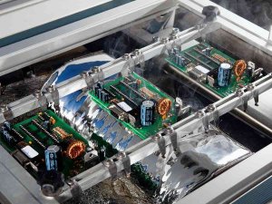
Flux removes oxidation layers and promotes wetting.
Types: Rosin-based (R/RA/RMA), water-based, and low-solids no-clean.
Application Methods: Foam-type (uniform but wasteful), spray-type (precise control), and ultrasonic atomization (high-end equipment).
Key Control Points: Application volume, uniformity, and the degree of flux activation after preheating.
Preheating Temperature Profile
Preheating removes solvents from the flux, activates the flux, and reduces thermal shock.
Parameters: Preheating temperature 80–130°C (lead-containing) or 100–150°C (lead-free); preheating time 1–3 minutes; temperature difference between the top and bottom of the PCB <100°C.
Wave Parameter Control
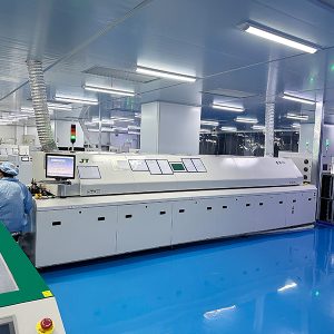
Wave height, speed, and angle determine soldering quality.
Key parameters: wave height (1/2 to 2/3 of PCB thickness), conveyor speed (1.0–1.5 m/min), tilt angle (5–7°), and tin temperature (250–265°C for lead-free).
Common Defects and Countermeasures
Bridging: Solder connections between adjacent leads. Countermeasures: Reduce wave height, increase the tilt angle, or use a solder-dragging pad design.
Pointed Tips: Sharp tips at the ends of solder joints. Countermeasures: Optimize the cooling rate and adjust the flux activity.
Pores: Voids inside the solder joint. Countermeasures: Control PCB moisture exposure, optimize preheating, and use nitrogen shielding.
Insufficient Solder: Pins are not fully covered. Countermeasures: Increase wave height, reduce conveyor speed, or check pin solderability.
Nitrogen Wave Soldering
Nitrogen shielding reduces oxidation and improves wettability.
Advantages: Reduces bridging and porosity, allows for lower flux usage, and improves yield in lead-free processes.
Cost: Nitrogen consumption increases operating costs by approximately 15–25%.
Wave soldering is a mature yet precise process. Fine-tuning parameters significantly affects yield; Standard Operating Procedures (SOPs) must be established and regularly validated.

Frequently Asked Questions (FAQ)
Q1: Can wave soldering and reflow soldering be performed on the same board?
A: Yes, this is known as a mixed-assembly process. Typically, SMT components are reflow soldered first, followed by wave soldering of THT components. Note that SMT components must be secured with red glue or positioned on the opposite side of the board from the wave soldering area to prevent them from falling off during wave soldering.
Q2: Why are lead-free wave soldering temperatures higher?
A: Lead-free solder paste has a melting point of 217°C, so wave soldering temperatures must be 250–265°C to ensure proper wetting. This is approximately 20–30°C higher than leaded wave soldering (230–250°C). Higher temperatures accelerate solder oxidation and copper corrosion, requiring more frequent solder pot maintenance and nitrogen protection.
Q3: Why must the PCB be tilted as it passes through the wave soldering process?
A: The tilt angle (5–7°) helps solder flow out from between the leads, reducing bridging. At the same time, gravity ensures even solder distribution. Too steep an angle results in insufficient solder, while too shallow an angle increases bridging.
Q4: Why does the copper content in the solder pot increase?
A: At high temperatures, copper from PCB pads and component leads dissolves into the molten solder. When the copper content exceeds 0.3% (lead-containing) or 0.7% (lead-free), solder flowability decreases and bridging increases. Copper content must be monitored regularly, and the solder should be diluted with pure tin or completely replaced as needed.
Q5: Can double-sided SMT boards be soldered using wave soldering?
A: Yes, but mounted components must be protected. Methods: 1) Position SMT components on the side opposite the wave soldering area; 2) Use a carrier to shield the SMT side; 3) Perform selective wave soldering to heat only the THT areas. Mixed-assembly boards with both SMT and THT components on both sides require careful process planning.
