
Moving from PCB prototyping assembly to full-scale mass production is one of the most critical transitions in electronics manufacturing. A well-executed PCB prototyping assembly phase lays the foundation for everything that follows. A design that works perfectly on a lab bench can fail spectacularly on a high-speed SMT line if the transition is not managed carefully. According to industry data, nearly 40% of electronic products experience delays during the prototype-to-production handoff, with the root causes ranging from component availability issues to manufacturability gaps that were never caught during the prototyping phase.
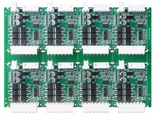
At Keep Best PCB Assembly, we have guided hundreds of clients through this transition. This guide distills the best practices we have learned into a practical framework that covers design optimization, component sourcing, process validation, documentation, and partner selection. Whether you are a startup shipping your first product or an established OEM scaling a new design, these principles will help you avoid costly delays and quality surprises.
1. Design for Manufacturability: Start Early, Iterate Often
The single biggest mistake teams make is treating DFM as a final checkbox rather than an ongoing conversation. When you engage a PCB assembly manufacturer during the prototyping phase, their engineering team can flag issues while design changes are still cheap. Waiting until the Gerber files are frozen means every revision costs time and money.
PCB Panelization and Tooling Considerations
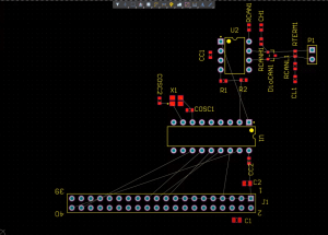
What works for a 5-board PCB prototyping assembly run rarely scales to a 5,000-unit production batch. Key panelization considerations include:
- V-score vs. tab-routing: V-scoring is faster and cheaper for rectangular boards, but tab-routing with mouse bites is necessary for irregular shapes or boards with overhanging components near the edge.
- Fiducial marks: At least three global fiducials on each panel, plus local fiducials near fine-pitch components. Prototypes often skip local fiducials, but automated optical inspection in production demands them.
- Tooling holes: Production carriers and fixtures require precise tooling hole placement. Add these to your design during prototyping so they are validated alongside your circuit.
- Panel utilization rate: Aim for at least 70% board area within the panel frame. Poor utilization at scale can double your per-unit cost. Addressing these factors during PCB prototyping assembly prevents expensive tooling changes later.
Component Selection for Production Scale
During PCB prototyping assembly, engineers often choose components based on datasheet specs alone, without considering the realities of mass production PCB assembly. Three factors demand attention:
1. Package standardization. During PCB prototyping assembly, that exotic QFN package with a 0.35 mm pitch might solder fine by hand, but it will push your SMT line’s capability limits and increase defect rates. Where possible, choose packages that are within your assembly partner’s standard process window. For fine-pitch devices, confirm that your partner has the paste printing and placement equipment to handle them reliably at volume.
2. Thermal pad and via design. Center thermal pads on QFN and DFN packages must have properly designed via patterns for solder evacuation. Without adequate thermal relief, voiding rates can exceed 25% on production runs. IPC-7093 and IPC-7095 provide detailed guidance on thermal pad design that should be followed from the first prototype revision.
3. Component height and keep-out zones. Wave soldering fixtures and selective soldering nozzles need clearance around through-hole components. A design that is too dense near connectors or tall capacitors will require expensive custom tooling.
2. Component Sourcing and Supply Chain Readiness
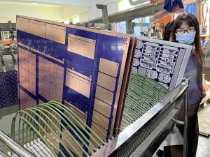
PCB prototyping assembly runs typically use distributor stock or sample quantities, but production volumes face entirely different supply dynamics. What was readily available during PCB prototyping assembly may have 26-week lead times at volume. Even a single unavailable component can halt an entire production line, and the cost of line stoppage far exceeds the cost of proactive sourcing.
Building a Production-Ready BOM
A prototype BOM often contains placeholders, single-source parts, and obsolete designators. During PCB prototyping assembly, engineers may tolerate these gaps, but they become production-stoppers at scale. Before committing to mass production PCB assembly, your BOM must be production-hardened:
- Full manufacturer part numbers (MPNs): Replace generic descriptions with exact MPNs. “10 µF 0603 capacitor” is not sufficient. Specify manufacturer, series, tolerance, voltage rating, and dielectric type.
- Approved alternates: Identify at least one qualified alternate for every active component, ideally from a different manufacturer to reduce single-source risk.
- Lifecycle status verification: Check every MPN against the manufacturer’s product change notification (PCN) database. Parts nearing end-of-life should be flagged and replaced before production begins.
- Minimum order quantity (MOQ) awareness: Some components have MOQs in the thousands. If your production volume is lower, identify distributors who can break reels or consider consignment arrangements.
A competent electronic manufacturing services provider will offer BOM scrubbing as part of their NPI service. This includes cross-referencing alternates, checking lifecycle status, and flagging long-lead-time items before they become emergencies. At Keep Best, our procurement team maintains relationships with over 500 component suppliers across Asia, giving us the flexibility to source even during shortages.
3. Process Validation: Bridge Prototype Quality to Production Metrics
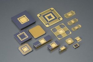
The quality expectations for PCB prototyping assembly are fundamentally different from those for production. A prototype run might tolerate manual rework on 10% of boards, but a production line targeting 98% first-pass yield cannot. Process validation closes this gap.
First Article Inspection (FAI)
Before committing a full production batch, run a first article build of 20 to 50 units on the actual production line. This step bridges the gap between PCB prototyping assembly validation and production-scale manufacturing. This serves several purposes:
- Verify the solder paste stencil: Confirm aperture sizes, thickness, and release characteristics on the production printer, not the prototype bench.
- Validate the reflow profile: Production ovens have different thermal characteristics than lab equipment. A profile that works on 5 boards may overheat component bodies on 500.
- Check placement accuracy: Fine-pitch and BGA components should be inspected via X-ray on the first article build to catch placement shifts before they propagate.
- Run full ICT/FCT: Prototypes often skip in-circuit testing, but production should not. The FAI is your opportunity to debug test fixtures and boundary-scan programs.
Testing Strategy from Prototype to Production
A layered testing strategy, established during PCB prototyping assembly and refined for production, ensures defects are caught at the earliest possible stage:
Level 1 — Automated Optical Inspection (AOI): Post-placement and post-reflow AOI catches solder bridging, tombstoning, missing components, and polarity errors. Modern 3D AOI systems can measure solder joint volume and detect lifted leads.
Level 2 — X-ray Inspection: Essential for BGA, QFN, and other hidden-joint packages. Production X-ray systems can be programmed to inspect every board or sampled statistically based on criticality.
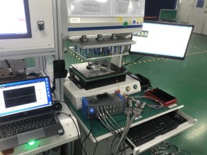
Level 3 — In-Circuit Testing (ICT): Verifies component values, orientation, and basic circuit integrity. Development of the ICT fixture and program should begin during the prototyping phase so it is ready for the first production run.
Level 4 — Functional Testing (FCT): Simulates real-world operating conditions to verify that the assembled board performs to specification. FCT is particularly important for box build assembly where the PCB integrates with enclosures, wiring harnesses, and electromechanical subsystems.
4. Documentation and Traceability
Production documentation is often an afterthought during PCB prototyping assembly, but it becomes the backbone of quality management at scale. Without proper documentation, scaling production across multiple lines or facilities becomes nearly impossible.
Key documentation deliverables include:
- Production work instructions: Begin drafting these during PCB prototyping assembly. Detailed visual guides for each assembly step, including solder paste application, component placement, hand-soldering touch-up, conformal coating, and final inspection criteria.
- Process control plans: Documented limits for solder paste inspection (SPI), reflow oven parameters, placement force, and all critical process variables.
- Traceability records: Even at the PCB prototyping assembly stage, a MES (Manufacturing Execution System) should track every board by serial number, recording which feeder loaded each component reel, which operator ran each shift, and which oven profile was active. This is essential for root-cause analysis when field failures occur and is a requirement for IATF 16949 and ISO 13485 certified production.
- Material certificates and CoCs: Certificates of Conformance for PCBs, components, solder paste, and consumables should be archived and linked to each production batch.

5. Choosing the Right Manufacturing Partner for Scale
Not every shop that handles PCB prototyping assembly can manage production volumes, and not every high-volume factory is equipped for the NPI handoff. The ideal partner for the prototype-to-production transition should offer a one-stop PCBA solution that spans engineering support, component procurement, SMT and through-hole assembly, testing, and box build integration.
When evaluating partners, consider these questions:
- Does the partner have dedicated NPI engineers? These specialists bridge the gap between your design team and the production floor. They review Gerber files for manufacturability, suggest component alternates, and develop the process flow before the first production board is built.
- What is the partner’s equipment capability? Ask about solder paste inspection resolution, placement machine accuracy, reflow oven zone count, and AOI/X-ray capability. The equipment that works for prototyping may not meet the throughput and precision demands of mass production PCB assembly.
- Does the partner offer in-house testing? Some assemblers outsource ICT and FCT, which adds turnaround time and reduces quality visibility. An in-house testing capability is a strong indicator of production maturity.
- Can the partner scale geographically? If your product will eventually ship to multiple regions, a partner with facilities in different countries, such as Shenzhen and Thailand, can reduce logistics costs and tariff exposure.
- What certifications does the partner hold? ISO 9001 is the baseline. If your product serves automotive, medical, or aerospace markets, look for IATF 16949, ISO 13485, or AS9100 certification respectively.
6. Production Ramp-up: The Pilot Build and Beyond
The pilot build is the final gate between PCB prototyping assembly and full production release. Unlike the FAI, which validates the process on a few dozen units, the pilot build typically runs 100 to 500 units and simulates the full production environment, including packaging, labeling, and shipment.
During the pilot build, pay attention to:
- Yield metrics: Target a first-pass yield of at least 95% on the pilot build. If yields are lower, pause and investigate before scaling further. Common culprits include inadequate stencil design, component moisture sensitivity, and reflow profile mismatches.
- Throughput and takt time: Measure actual cycle time against the production plan. Bottlenecks at manual inspection stations, programming steps, or packaging often surface during the pilot build.
- Operator training effectiveness: Production operators should be able to follow work instructions without engineer supervision. If they cannot, the documentation needs improvement.
- Supply chain performance: Track on-time delivery of every component line item. Even 95% on-time delivery for a 100-line BOM means 5 components are late, any one of which can stop the line.
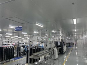
Once the pilot build passes all gates with acceptable yields, throughput, and documentation, the line is cleared for full mass production PCB assembly. Ongoing statistical process control (SPC) and regular audits maintain the quality baseline established during NPI.
Conclusion
The transition from PCB prototyping assembly to mass production is not a single event but a phased process spanning DFM optimization, supply chain hardening, process validation, documentation, and partner selection. Companies that treat this transition as a collaborative engineering exercise, rather than a simple handoff of Gerber files, consistently achieve faster time-to-market, higher first-pass yields, and lower total cost of quality.
For companies navigating the shift from PCB prototyping assembly to mass production, choosing the right partner is the single most impactful decision. At Keep Best PCB Assembly, our NPI team works alongside your engineers from the first prototype through full production ramp-up, providing DFM feedback, BOM scrubbing, and process validation at every stage of PCB prototyping assembly and production. With three manufacturing facilities in Shenzhen, Jiangmen, and Thailand, we offer the scale and geographic flexibility to support your product through its entire lifecycle. Contact Keep Best PCBA for professional support on your next prototype-to-production transition.
