
Mass Production PCB Assembly: Quality Control Guide for 2026
When production volumes scale from hundreds to tens of thousands of boards per month, mass production PCB assembly demands a fundamentally different quality approach than prototyping. A 0.5% defect rate that seems acceptable on a 100-unit pilot run translates into 500 field failures at 100,000 units. Leading manufacturers solve this by building layered quality control systems on top of international standards, statistical process control, and automated inspection technologies.
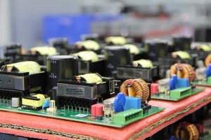
This guide explains how mass production PCB assembly teams maintain consistent quality at scale — from ISO-certified process frameworks to real-time defect detection and full MES traceability. Whether you are scaling from NPI to volume ramp or evaluating a new PCB assembly manufacturer, these quality systems determine whether your boards perform reliably in the field.
How ISO Standards Govern Mass Production Quality
International standards provide the structural backbone for mass production PCB assembly quality. ISO 9001 establishes the baseline quality management system (QMS), requiring documented procedures, corrective action loops, and regular management reviews. For high-volume electronic manufacturing services, this foundation is non-negotiable.
Beyond ISO 9001, industry-specific certifications add deeper rigor depending on the end product:
- IATF 16949 — Governs automotive electronics with emphasis on PPAP (Production Part Approval Process), FMEA, and proactive defect prevention
- ISO 13485 — Adds design controls, risk management, and CAPA (Corrective and Preventive Action) for medical device assembly
- IPC J-STD-001 — Defines solder joint acceptability standards applied on every production line
- IPC-A-610 — Provides visual inspection criteria for both operator and automated inspection stations
PPAP and First Article Approval
In automotive and industrial mass production PCB assembly, PPAP locks the manufacturing process before volume builds begin. The supplier submits documentation proving that the process, materials, and inspection methods consistently produce conforming parts. Once approved, any change — component substitution, reflow profile adjustment, or stencil modification — triggers a new PPAP submission. This prevents unauthorized process drift that could compromise quality at scale.

Statistical Process Control on the SMT Line
SPC transforms quality from reactive inspection to proactive process management. In mass production PCB assembly, critical parameters are monitored continuously using control charts rather than waiting for end-of-line failures:
- Solder paste volume — Measured by SPI (Solder Paste Inspection) at each pad position
- Reflow temperature profile — Verified against a golden profile at each shift change
- Component placement offset — Tracked from pick-and-place machine telemetry
- Defects per million opportunities (DPMO) — Calculated at AOI stations and reviewed daily
The key metric is Cpk (process capability index). A Cpk of 1.33 is the minimum threshold for most production environments, while automotive and medical applications often require Cpk greater than or equal to 1.67. When a parameter drifts toward control limits, operators intervene before defects occur — this prevention-over-detection principle is what separates mature mass production PCB assembly operations from amateur shops.
Control Chart Interpretation
Western Electric rules help identify out-of-control conditions: a single point beyond 3-sigma, two of three consecutive points beyond 2-sigma, or eight consecutive points on one side of the centerline. In modern mass production PCB assembly, these rules are applied automatically by MES software, triggering alerts before a process excursion becomes a defect trend that reaches the customer.
Layered Automated Inspection Strategy
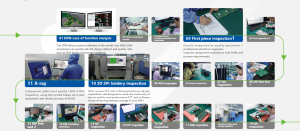
No single inspection method catches every defect type. Mass production PCB assembly lines use a layered approach where each station targets specific failure modes, creating overlapping coverage that drives total escape rates toward zero.

SPI — Solder Paste Inspection
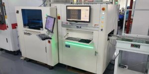
3D SPI measures paste volume, height, and area on every pad before components are placed. Since 60-70% of SMT defects originate from solder paste printing, this station provides the earliest possible defect detection point. High-volume SMT assembly services typically set paste volume limits at plus or minus 30% of target, with tighter plus or minus 20% limits for fine-pitch and BGA components.
3D AOI — Automated Optical Inspection
Post-reflow AOI inspects solder joint quality, component presence, polarity marks, and placement accuracy. 3D AOI adds height measurement, catching lifted leads and tombstoning defects that 2D systems miss. In mass production PCB assembly, AOI runs at 100% inspection coverage with defect classification data feeding back to upstream process control for continuous improvement.
X-Ray Inspection for Hidden Joints
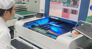
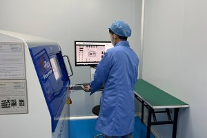
X-ray inspection reveals defects invisible to optical systems: BGA voiding, QFN solder coverage, and through-hole barrel fill percentage. For BGA-heavy assemblies common in consumer electronics, X-ray inspection is mandatory at production volume. Automated X-ray (AXI) systems inspect 100% of joints on high-value boards or use statistical sampling for lower-risk product families.
ICT and Functional Testing
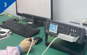
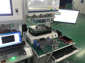
In-circuit testing (ICT) verifies individual component values, shorts, and opens, while functional testing (FCT) validates board-level performance under operating conditions. In mass production PCB assembly, test coverage is balanced against cycle time — ICT typically covers 85-95% of nodes, with FCT catching system-level integration issues that component-level tests cannot detect.
AQL Sampling Plans and Acceptance Criteria
While automated inspection covers 100% of solder joints, certain attributes — cosmetic defects, conformal coating coverage, and label legibility — are verified through sampling. Acceptance Quality Limit (AQL) sampling plans define how many units to inspect and how many defects are allowable before a lot is rejected.
Common AQL levels applied in mass production PCB assembly:
- Level II (General inspection) — Critical defects: 0, Major defects: 0.65%, Minor defects: 1.0%
- Level I (Relaxed) — Critical defects: 0, Major defects: 1.0%, Minor defects: 2.5%
- Special S-4 (Reduced sampling) — Critical defects: 0, Major defects: 0.65%, Minor defects: 1.0%
If a lot fails AQL sampling, the entire batch is 100% re-inspected or scrapped depending on defect severity. This is why prevention through SPC is always cheaper than relying on post-hoc sampling — a single rejected lot can wipe out the cost savings of an entire production run.
MES Traceability for Volume Production
Modern mass production PCB assembly runs on Manufacturing Execution Systems (MES) that track every board through every process step. Traceability is not just about recall readiness — it is the foundation of root cause analysis and data-driven continuous improvement.
A robust MES records the following data points for every single board:
- Board serial number — Laser-marked or barcode-labeled at the start of the line
- Component lot codes — Linked to each placement position on the board
- Process parameters — Reflow profile, paste batch number, stencil ID per board
- Inspection results — SPI, AOI, X-ray, ICT, and FCT data linked by serial number
- Operator and shift — Who ran each station and when, for accountability
When a field failure occurs, the MES genealogy trace identifies the exact boards produced with the same component lot, reflow profile, or paste batch — enabling targeted recalls rather than blanket returns. In automotive and medical environments served by a one-stop PCBA solution provider, this traceability depth is a regulatory requirement, not a nice-to-have.
Selecting a Mass Production PCB Assembly Partner
Scaling to volume production requires a partner with proven quality systems, not just SMT equipment on the floor. Any contract electronics manufacturer can place components, but maintaining consistent quality across 100,000-unit runs demands embedded process discipline. Evaluate these seven factors before committing your production volume:
- Certification scope — Verify ISO 9001, IATF 16949, or ISO 13485 are current and cover the specific manufacturing site
- SPC implementation — Ask to see live control charts and Cpk data from current production runs
- Inspection coverage — Confirm SPI, 3D AOI, X-ray, and ICT/FCT capabilities are available on-site, not outsourced
- MES traceability — Request a demonstration of board genealogy lookup and recall scope simulation
- DPMO track record — Benchmark their historical defect rates against industry standards for your product type
- FAI process — Review their first article inspection documentation format and turnaround time
- Capacity and scalability — Ensure the line can handle your forecasted volumes without compromising quality or lead time
Common Quality Pitfalls at Production Scale
Several specific issues emerge when scaling from prototype to mass production PCB assembly. Being aware of these pitfalls helps you ask the right questions during supplier audits:
- Stencil wear — After 50,000-plus prints, aperture edges dull and cause paste volume drift. Proactive stencil replacement schedules based on print count prevent this
- Component placement drift — Long production runs can shift feeder alignment. Regular feeder calibration every shift prevents systematic placement errors
- Reflow profile aging — Oven belt speed and zone temperatures drift over time. Verify the profile against a golden board weekly at minimum
- AOI false accept rates — Programs tuned for maximum sensitivity generate excessive false rejects, tempting operators to override calls. Balance sensitivity with practical false-call rates below 5%
Each of these pitfalls is preventable when the manufacturer maintains mature SPC, scheduled preventive maintenance, and a culture of data-driven process management rather than reactive firefighting.
Conclusion
Quality in mass production PCB assembly is not achieved by inspecting harder — it is engineered into the process through standards, statistics, and automation. ISO-certified QMS frameworks provide the structure, SPC provides early warning of process drift, layered inspection catches what slips through, and MES traceability ensures accountability from bare board to shipped product.
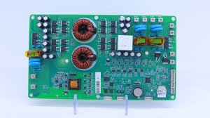
When every process parameter is monitored, every defect is classified and fed back upstream, and every board is fully traceable, defect rates below 1,000 DPMO become achievable — even at volumes exceeding 100,000 units per month. Contact Keep Best PCBA for professional mass production PCB assembly services backed by ISO 9001, IATF 16949, and ISO 13485 certifications, 3D AOI and X-ray inspection capabilities, and full MES traceability across our Shenzhen and Thailand manufacturing facilities.