
IoT PCB Assembly: Smart Factory Manufacturing Guide for 2026
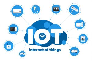
The rapid expansion of connected devices has placed IoT PCB assembly at the center of modern electronics manufacturing. From smart home sensors to industrial monitoring systems, IoT products demand specialized assembly processes that combine miniaturization, wireless integration, and rigorous quality control. As the Internet of Things ecosystem grows beyond 30 billion connected devices worldwide, manufacturers are turning to smart factory technologies to meet the volume, reliability, and cost targets that IoT applications require. This guide examines how IoT PCB assembly differs from conventional PCBA, the smart factory innovations driving it forward, and what electronics brands need to know when selecting a manufacturing partner for connected device production.
What Makes IoT PCB Assembly Different
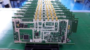
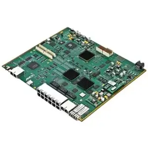
IoT devices combine sensing, processing, wireless communication, and power management within extremely compact enclosures. This convergence creates manufacturing requirements that go well beyond standard consumer electronics assembly. An IoT PCB assembly typically involves mixed-signal circuitry, RF modules, and ultra-low-power components on the same board, all while maintaining signal integrity across multiple frequency bands.
Several characteristics distinguish IoT PCB assembly from traditional PCBA:
- High-density interconnect (HDI) requirements: Most IoT products use 0201 or even 01005 passive components, fine-pitch BGAs, and blind/buried vias to achieve compact form factors
- Wireless module integration: Wi-Fi, Bluetooth, Zigbee, LoRa, and NB-IoT modules must be soldered and tested for RF performance during assembly
- Mixed-signal complexity: Analog sensor interfaces and digital processing circuits coexist on the same PCB, requiring careful layout and soldering control
- Low-power constraints: Sleep-mode current consumption demands clean solder joints and minimal flux residue to prevent parasitic leakage
- Conformal coating: Many IoT devices operate outdoors or in humid environments, making protective coating a standard step in IoT PCB assembly
These factors mean that a factory capable of standard PCBA may not automatically qualify for IoT PCB assembly without additional process controls, equipment, and expertise.
Smart Factory Technologies Transforming IoT PCB Assembly
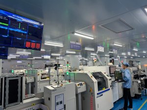
The concept of a smart factory—where machines communicate, data flows in real time, and AI algorithms optimize production—has become especially relevant to IoT PCB assembly. The high volume, tight tolerances, and quality expectations of connected device manufacturing demand a level of automation and intelligence that manual processes cannot deliver.
AI-Driven Process Control
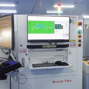
Modern IoT PCB assembly lines use artificial intelligence at multiple inspection stages. AI-powered solder paste inspection (SPI) systems analyze stencil printing quality in three dimensions, flagging insufficient paste, bridging, or misalignment before components are placed. This early defect catch prevents costly rework downstream.
Similarly, 3D automated optical inspection (3D AOI) machines equipped with deep learning algorithms can distinguish between acceptable solder joint variations and genuine defects. For IoT PCB assembly, where 0201 components and 0.4mm pitch packages are common, this level of discrimination is essential. AI models trained on thousands of defect images continuously improve their accuracy, reducing false reject rates and catching subtle defects that human inspectors might miss.
Digital Twin Simulation
A digital twin is a virtual replica of the physical production line. In IoT PCB assembly, digital twins simulate the entire manufacturing process—from solder paste application through reflow and inspection—before a single board enters production. Engineers can test reflow profiles, component placement sequences, and stencil aperture designs in the virtual environment, identifying potential issues without consuming materials or machine time.
This capability is particularly valuable for new product introduction (NPI) in IoT PCB assembly, where time-to-market pressures demand rapid process validation. By simulating thermal profiles and predicting defect probabilities, digital twins reduce the number of physical iterations needed to achieve first-pass yield targets.
MES-Enabled Full Traceability
A Manufacturing Execution System (MES) serves as the digital backbone of a smart factory. For IoT PCB assembly, MES provides end-to-end traceability that records every process parameter, material lot, operator action, and inspection result associated with each board.
This traceability matters because IoT devices often enter critical applications—smart grid monitoring, medical wearables, industrial safety systems—where field failure can have serious consequences. When a defective unit is returned, MES records allow manufacturers to trace the root cause back to a specific solder paste lot, reflow oven zone, or component reel. This capability distinguishes a mature IoT PCB assembly operation from a basic assembly shop.
Key Design and Manufacturing Challenges
HDI Miniaturization
IoT products increasingly rely on high-density interconnect technology to pack more functionality into smaller footprints. HDI PCBs feature blind and buried vias, sequential lamination, and microvia routing that require specialized drilling and plating processes. During IoT PCB assembly, the smaller pad sizes associated with HDI designs create challenges for solder paste printing, component placement accuracy, and reflow profile optimization.
Stencils for IoT boards often require electroformed nickel apertures with nanocoatings to achieve clean paste release at 0201 and 01005 component pitches. The pick-and-place equipment must maintain placement accuracy within 25 microns or better, demanding regular calibration and vision system optimization.

RF and Antenna Integration
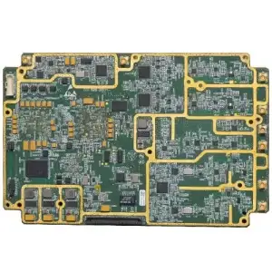
Wireless connectivity is a defining feature of IoT devices, and antenna performance depends heavily on PCB design and assembly quality. RF module assembly requires controlled solder volumes to maintain impedance matching, and antenna matching circuits must be tuned after assembly to account for parasitic effects introduced by solder and substrate properties.
In IoT PCB assembly, RF testing is often performed at the functional test stage using over-the-air (OTA) chamber measurements to verify radiated performance. This adds a test step not typically found in conventional PCBA, and it requires specialized equipment and shielding environments.
Power Management and Battery Constraints
IoT devices are designed for long battery life, which means their power management circuits must operate with minimal quiescent current. Poor solder joints, flux residue, or contamination from the IoT PCB assembly process can introduce parasitic resistance or leakage paths that drain batteries prematurely. Clean assembly processes—using no-clean or low-residue flux formulations, thorough cleaning where specified, and ionic contamination testing—are essential for meeting IoT power consumption targets.

Quality Assurance for IoT Connected Devices
Quality assurance in IoT PCB assembly goes beyond visual inspection. Connected devices must perform reliably in diverse environments, often without physical access for maintenance. A comprehensive quality strategy combines multiple inspection and testing methods.
3D AOI and X-Ray Inspection
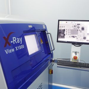
Three-dimensional AOI captures height data for every solder joint, enabling detection of insufficient solder, lifted leads, and tombstoning defects that 2D inspection cannot reliably identify. For BGA and QFN packages common in IoT designs, X-ray inspection verifies solder joint formation beneath the package, checking for voiding, bridging, and head-in-pillow defects.
Functional and Connectivity Testing
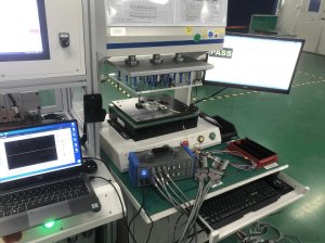
Functional testing for IoT devices typically includes:
- In-circuit testing (ICT): Verifies individual component values and short/open conditions
- Functional testing (FCT): Powers up the board and tests core operating functions
- RF performance testing: Measures wireless parameters including output power, receiver sensitivity, and frequency accuracy
- Boundary scan testing: Tests interconnections between digital ICs using JTAG
- Burn-in testing: Subject boards to elevated temperature and voltage stress to screen for early-life failures
This multi-layered testing approach ensures that each IoT PCB assembly meets both electrical and wireless performance specifications before it ships to the end customer.
Industry 4.0 Trends Shaping IoT PCB Assembly
The Industry 4.0 movement is reshaping how IoT PCB assembly facilities operate. Several emerging trends are worth watching:
- Predictive maintenance: AI algorithms monitor equipment health data to predict failures before they occur, reducing unplanned downtime on high-volume IoT assembly lines
- Collaborative robots: Cobots handle repetitive tasks like component tray feeding and board transfer, freeing human operators for quality-critical activities
- Cloud-based production analytics: Real-time dashboards give manufacturers visibility into yield, cycle time, and defect trends across multiple IoT PCB assembly lines and facilities
- Smart materials tracking: RFID-tagged component reels and barcoded stencils enable automatic material verification, reducing the risk of wrong-part placement
- Adaptive process optimization: Machine learning models analyze process data in real time, automatically adjusting reflow profiles and placement parameters to maintain yield targets
These technologies are not theoretical—they are being deployed in leading IoT PCB assembly facilities today, and their adoption will accelerate as connected device volumes continue growing.
How to Choose an IoT PCB Assembly Partner
Selecting the right manufacturing partner for IoT devices requires evaluating capabilities that go beyond standard PCBA metrics. Consider these factors when assessing an IoT PCB assembly provider:
- Smart factory maturity: Does the factory use AI-driven SPI, 3D AOI, and MES traceability? Are production data available to customers in real time?
- RF and wireless expertise: Can the partner demonstrate experience with Wi-Fi, Bluetooth, LoRa, and other wireless module assembly and testing?
- HDI capability: Does the facility have equipment and processes qualified for 0201/01005 components and fine-pitch BGA placement?
- Cleanroom or controlled environment: For IoT devices with conformal coating or contamination-sensitive applications, is a controlled environment available?
- Testing infrastructure: Does the partner offer ICT, FCT, RF testing, and burn-in capabilities under one roof?
- Certifications: Look for ISO 9001, IATF 16949, or ISO 13485 depending on your industry, and verify that the quality management system covers IoT-specific processes
- Prototype-to-production scalability: Can the partner support low-volume pilot builds and scale to mass production without process requalification?
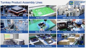
A partner like Keep Best PCBA, with dual manufacturing bases in China and Thailand, 15+ SMT lines equipped with 3D AOI and X-ray inspection, and MES-enabled traceability, offers the combination of innovation, scale, and quality discipline that IoT PCB assembly demands. As a PCB assembly manufacturer serving global electronics brands, the company combines one-stop PCBA solution capabilities with Industry 4.0 technologies to deliver connected device manufacturing at competitive cost and reliable quality.
Conclusion
IoT PCB assembly represents a convergence of miniaturization, wireless integration, and smart factory innovation. As connected devices continue penetrating industrial, consumer, and infrastructure markets, the manufacturing processes behind them must evolve to meet higher quality, traceability, and efficiency standards. By leveraging AI-driven inspection, digital twin simulation, MES traceability, and multi-layered testing, leading manufacturers are building the foundation for reliable IoT production at scale. For brands developing connected products, choosing an IoT PCB assembly partner with proven smart factory capabilities is the surest path to market success in 2026 and beyond. Contact Keep Best PCBA to discuss your IoT device manufacturing requirements and discover how smart factory technology can accelerate your time-to-market while ensuring production quality.