
Even the most advanced PCBA facilities generate defects. The difference between a supplier you trust and one you fire is not whether errors occur — it is how thoroughly those errors are intercepted before boards reach your hands. This field guide examines the ten most persistent faults in printed circuit board assembly, their root mechanisms, and the proven countermeasures that prevent them from becoming field failures.
Defect 1: Solder Bridging — The Unwanted Short
What You See: Two adjacent conductive pads, meant to remain electrically isolated, are joined by an accidental thread of solder. The result is a short circuit that can destroy integrated circuits, drain batteries, or trigger thermal runaway.
Why It Happens:
- Stencil apertures oversized relative to pad dimensions, extruding paste onto solder mask
- Insufficient clearance between fine-pitch leads (typically below 0.5 mm pitch)
- Reflow peak temperature overshoot causing uncontrolled solder flow
- Board flexure during heating, squeezing molten solder sideways between pads
How to Prevent It:
- Apply the 0.66 area ratio rule for aperture design — never exceed paste volume that the pad can physically contain
- For QFPs below 0.5 mm pitch, use home-plate or inverted home-plate aperture shapes that reduce paste at toe and heel regions prone to bridging
- Maintain rigid board support through reflow to prevent Z-axis warping beyond 1% of board diagonal length
- Calibrate reflow oven zone temperatures weekly to prevent hot spots
Defect 2: Cold Solder Joints — The Weak Connection
What You See: A solder joint appears grainy, dull, or exhibits a rough surface texture rather than the smooth concave meniscus of a properly wetted connection. Both mechanical strength and electrical conductivity suffer.
Why It Happens:
- Reflow profile insufficient in peak temperature or dwell time for the specific alloy (lead-free SAC305 demands 235–250°C peaks versus 210–230°C for legacy tin-lead)
- Oxidized component leads or PCB pads, especially on immersion tin or bare copper finishes stored beyond shelf life
- Solder paste expired or improperly stored — flux activity degrades with time and temperature cycling
- Inadequate preheat causing thermal shock rather than gradual temperature ramp
How to Prevent It:
- Profile the actual board with thermocouples attached to critical components — never rely on oven setpoints alone
- Implement FIFO (first-in-first-out) paste inventory with strict 6-month refrigerated shelf life enforcement
- Specify PCB surface finish compatibility: ENIG (electroless nickel immersion gold) for long storage, OSP (organic solderability preservative) for cost-sensitive quick-turn projects
- Maintain reflow preheat ramp between 0.5–1.5°C per second through the 100–150°C range
Defect 3: Tombstoning — The Standing Component
What You See: A tiny rectangular resistor or capacitor stands vertically on one pad, resembling a miniature grave marker. Only one terminal connects; the other floats in air, creating an open circuit.
Why It Happens:
- Asymmetric solder paste volume between the two pads — even a 10% difference can create unequal wetting forces
- Dissimilar pad sizes or thermal mass on opposite ends, causing one side to reach liquidus temperature before the other
- Component body offset from pad centers, shifting the wetting force vector
- Excessive reflow ramp rate (above 2°C per second) exaggerating thermal asymmetry
How to Prevent It:
- Enforce symmetric pad geometry for 0402 and smaller components — matching dimensions within ±0.025 mm
- For critical applications, specify thermal relief patterns that equalize heat sinking to both pads
- Keep reflow preheat ramp between 0.5–1.5°C per second to minimize thermal gradients across small passives
- Consider nitrogen reflow atmosphere to reduce the wetting time differential that drives tombstoning
Defect 4: Missing Components — The Empty Pads
What You See: A placement program called for a capacitor. The BOM lists a capacitor. The schematic needs a capacitor. The board shows bare copper pads where the capacitor should sit.
Why It Happens:
- Vacuum nozzle on the placement head failed to generate sufficient negative pressure — component dropped during transit from feeder to board
- Tape-and-reel pocket empty or component stuck in cover tape; machine continued without error detection
- Component mapped to wrong feeder position in the placement program
- Board transported upside-down or jolted after placement but before reflow
How to Prevent It:
- Implement component presence verification at the placement head — vacuum pressure sensors or vision confirmation before board indexing
- AOI (Automated Optical Inspection) after placement station, before reflow, catches missing components while they are still correctable
- Reel change protocols with barcode verification — never rely on human memory for component identity
- Anti-vibration transport carriers between placement and reflow ovens
Defect 5: Wrong Component or Reversed Polarity
What You See: The board powers on but behaves erratically. Hours of debugging trace the issue to a 4.7 kΩ resistor where the design specified 47 kΩ — or a Schottky diode installed backward, blocking current that should flow freely.
Why It Happens:
- Reels with similar component body markings loaded into incorrect feeder slots
- Human kitting error during assembly setup, especially with components sharing identical packages (0402 resistors and capacitors look identical to the naked eye)
- Polarity indicators (dot, stripe, bevel) misinterpreted or poorly visible on tiny packages
- No systematic first-article comparison between physical board and Bill of Materials
How to Prevent It:
- Component reel barcode scanning at feeder loading — software validates part number against BOM before machine acceptance
- First-article inspection with magnified photography of every unique component, stored as the production reference standard
- DFM (Design for Manufacturability) review ensuring silkscreen polarity markings align unambiguously with component orientation indicators
- For high-value or safety-critical boards, implement ICT verification that measures actual resistor values and diode forward voltage drop
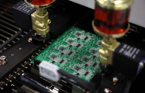
Defect 6: BGA and QFN Voiding — The Hidden Failure
What You See: From the outside, the BGA package looks flawless. Underneath, solder balls contain voids (gas pockets) exceeding 25% of joint area, or worse — completely unsoldered columns creating open circuits invisible to optical inspection.
Why It Happens:
- Moisture trapped in PCB or component materials outgasses during reflow, bubbling through molten solder
- Oxidized solder spheres or PCB pads preventing full wetting
- Insufficient peak temperature or short time above liquidus for large thermal mass packages
- PCB warpage creating variable standoff heights across the BGA array
How to Prevent It:
- Mandatory X-ray inspection** for every BGA assembly — this is non-negotiable for any quality-focused manufacturer
- Pre-bake PCBs at 125°C for 4–24 hours (depending on thickness) and moisture-sensitive components before assembly
- Nitrogen reflow atmosphere to minimize oxide formation on molten solder surfaces
- Board warpage measurement before and during reflow — keep below 0.75% to prevent corner joint opens
Defect 7: Solder Balling — The Migrating Spheres
What You See: Tiny spherical solder droplets, some smaller than grains of sand, scattered across the board surface. If they migrate under fine-pitch components, they create shorts that are nearly impossible to locate visually.
Why It Happens:
- Moisture absorption in solder paste causing explosive outgassing during rapid preheat
- Excessive preheat ramp rate (above 3°C per second) boiling volatile flux components before they can vent gradually
- Paste squeeze-out beneath stencil due to excessive squeegee pressure or poor board-to-stencil gasketing
- Slump in paste viscosity during warm ambient conditions before reflow
How to Prevent It:
- Paste storage at 0–10°C with 4-hour room-temperature equilibration before opening (never force-thaw in warm environments)
- Reflow preheat ramp strictly controlled to 1–2°C per second through the 100–150°C range
- Stencil-to-board gasketing verification — gaps as small as 0.05 mm cause paste leakage and subsequent balling
- Print pressure optimized for paste rheology — typically 0.5–1.0 kg per 25 mm of squeegee blade length
Defect 8: Pad Lifting and Trace Fracture — Structural Collapse
What You See: During functional testing or field operation, a copper pad detaches from the fiberglass substrate, or a trace cracks under thermal or mechanical stress. The electrical connection is permanently severed.
Why It Happens:
- Excessive rework temperature or dwell time during hand-soldering repairs, degrading epoxy-copper adhesion
- Mechanical flexure during handling, ICT fixture insertion, or assembly into enclosures
- Insufficient copper peel strength specified during PCB procurement (should exceed 1.05 N/mm per IPC-6012)
- Thermal cycling beyond design limits — CTE (coefficient of thermal expansion) mismatch between copper and substrate creates fatigue
How to Prevent It:
- Rework procedures with thermocouple-monitored tip temperature, never exceeding 350°C for more than 3 seconds per joint
- Board handling protocols prohibiting flexure beyond 1% of board diagonal
- Procurement specification: IPC-6012 Class 2 (general industrial) or Class 3 (high reliability) with documented copper peel test results
- Design practices: avoid 90-degree trace corners (use rounded), maintain adequate annular ring (minimum 0.05 mm), and anchor high-stress traces with teardrop pads
Defect 9: Insufficient Solder — The Starved Joint
What You See: A joint with visibly insufficient solder volume appears concave or hollow rather than convex and full. The connection may conduct initially but fails under vibration, thermal cycling, or mechanical load.
Why It Happens:
- Stencil aperture partially clogged with dried paste or debris — common with fine apertures below 0.3 mm
- Incomplete paste release from stencil walls due to poor area ratio (below 0.66) or insufficient squeegee pressure
- Component lead not seating into paste due to coplanarity issues (leads not all on the same plane)
- Paste drying before reflow because of excessive time between print and oven entry (above 4 hours in dry climates)
How to Prevent It:
- Automated stencil cleaning cycles between prints — ultrasonic or wipe-clean systems
- 3D SPI (Solder Paste Inspection) immediately after printing to flag low-volume deposits before placement commits them
- Incoming component inspection for lead coplanarity on QFPs and connectors — reject lots exceeding 0.05 mm variation
- Controlled assembly environment: 40–60% relative humidity, 20–26°C ambient to maximize paste working life
Defect 10: Ionic Contamination — The Invisible Corrosive
What You See: White crystalline or brown sticky residue surrounds solder joints. Even when invisible to the naked eye, ionic contamination from inadequate cleaning creates leakage currents, dendritic growth between traces, and eventual corrosion.
Why It Happens:
- No-clean flux residue not properly polymerized during reflow, leaving activators that absorb atmospheric moisture
- Water-soluble flux inadequately rinsed, leaving ionic salts on the board surface
- Human contamination during handling — skin oils, cosmetics, or industrial airborne contaminants
- Improper cleaning chemistry or incomplete drying after aqueous cleaning
How to Prevent It:
- Match flux classification to cleaning capability: no-clean for assemblies that will not be cleaned, water-soluble for assemblies with robust aqueous cleaning lines
- Ionic contamination testing per IPC-TM-650 method 2.3.25 — acceptable levels vary from below 1.5 μg NaCl equivalent per cm² (military/aerospace) to below 3.1 μg/cm² (consumer/industrial)
- Cleanroom-grade handling: nitrile gloves, ESD-safe tweezers, and controlled atmosphere storage
- Consider conformal coating for high-impedance or harsh-environment applications, applied only after cleaning validation passes
Detection Methods: Matching Each Defect to the Right Inspector
| Defect Category | Primary Detection Method | Secondary Confirmation |
| Solder bridging | AOI post-reflow | Visual microscopy at 10–40× magnification |
| Cold joints | AOI + ICT | Cross-sectional microanalysis |
| Tombstoning | AOI post-reflow | Visual inspection with magnification |
| Missing components | AOI post-placement | AOI post-reflow double-check |
| Wrong component / polarity | AOI + first-article inspection | ICT parametric value verification |
| BGA/QFN voids | 2D or 3D X-ray inspection | Destructive cross-section for validation |
| Solder balls | AOI + visual sweep | Ion chromatography if contamination suspected |
| Pad lifting | Visual inspection + bend testing | Microsection analysis of failed samples |
| Insufficient solder | 3D SPI + AOI | X-ray for hidden joints under large components |
| Flux residue | Visual + UV fluorescence | Ionic contamination meter (OMEGA meter) |
The Quality Philosophy: Layered Defense, Not Single Checkpoint
A single inspection gate is theater, not security. Effective PCBA quality relies on cumulative layers:
Layer 1 — Design Prevention: DFM reviews that eliminate tombstone-prone pad geometries, specify adequate clearances, and select appropriate surface finishes before a single board is ordered.
Layer 2 — Process Control: Real-time monitoring of paste print volume, placement accuracy, and reflow thermocouple data. Statistical process control (SPC) charts flag drift before it generates defects.
Layer 3 — Automated Optical Inspection: Post-placement and post-reflow cameras catch the obvious: missing, skewed, or wrong components; solder bridges; and gross solder anomalies.
Layer 4 — Radiographic Penetration: X-ray sees what cameras cannot — the hidden world under BGAs, QFNs, and connectors where the most expensive failures originate.
Layer 5 — Electrical Verification: ICT isolates component-level parametric failures; FCT validates that the entire circuit performs its mission.
Layer 6 — Environmental Proving: Burn-in, thermal cycling, and humidity exposure accelerate aging to catch infant-mortality failures before customers do.
Frequently Asked Questions About PCBA Defects
What is the most common PCBA defect?
Solder bridging and insufficient solder are among the most frequent defects, often originating from stencil design errors or paste printing inconsistencies. These are usually caught by AOI before boards ship.
Can all PCBA defects be detected before shipping?
No inspection system is 100% effective. However, a facility implementing SPI + AOI + X-ray + ICT + FCT can intercept the vast majority of defects. The remaining “escapees” typically fall below 50 parts per million in mature operations.
What does “PPM” mean in PCBA quality?
PPM stands for Parts Per Million, a standard metric for defect rates. A rate of 500 PPM means 0.05% of components or boards have defects. World-class manufacturers target below 100 PPM for mature products.
How much does rework cost compared to prevention?
Industry data suggests that catching a defect during paste printing costs approximately $0.50. Catching it during AOI costs $5. Reworking a board after final test costs $50–$200. A field failure costs $500–$5,000+ including warranty, logistics, and reputation impact. Prevention is always cheaper.
Should I accept a manufacturer that does not use X-ray inspection?

For any board containing BGAs, QFNs, or other hidden-joint components, X-ray inspection is mandatory. A manufacturer claiming AOI is sufficient for these packages is either technically uninformed or deliberately cutting corners. Neither is acceptable.
The defects described here are not theoretical textbook entries. They appear on production floors daily, in facilities ranging from garage operations to billion-dollar fabs. The difference between a supplier you trust and one you replace is not whether defects occur — it is whether those defects escape into your supply chain. Ask your manufacturer which of these six quality layers they implement. Their answer will reveal everything about their priorities. At keepbest, we apply all six layers as standard practice rather than optional upgrades.