
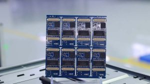
The electronics manufacturing industry has undergone a fundamental shift since the European Union introduced the Restriction of Hazardous Substances (RoHS) directive in 2006. Today, lead-free PCB assembly is not merely a regulatory checkbox — it represents a comprehensive engineering discipline that touches every stage of the production lifecycle, from solder paste selection to final inspection. As a contract electronics manufacturer serving global brands, Keep Best PCBA has integrated lead-free processes across all three manufacturing facilities in Shenzhen, Jiangmen, and Thailand, ensuring that every board meets international compliance standards without compromising reliability.
Why Lead-Free PCB Assembly Matters in Modern Electronics
Lead-free soldering replaces traditional tin-lead (SnPb) alloys with alternatives such as SAC305 (96.5% tin, 3.0% silver, 0.5% copper) and SN100C (tin-nickel-cobalt). In lead-free PCB assembly, this transition was initially driven by environmental regulations, but the benefits extend far beyond compliance. Lead-free solder joints withstand higher operating temperatures, resist tin pest formation in cold environments, and align with the sustainability goals that Fortune 500 companies now mandate across their supply chains.
However, the switch to lead-free alloys introduces distinct manufacturing challenges. The melting point of SAC305 (approximately 217°C) is roughly 34°C higher than that of eutectic SnPb solder (183°C). This elevated temperature profile demands tighter thermal management during reflow, more robust substrate materials, and enhanced process controls to prevent defects such as tombstoning, voiding, and intermetallic compound brittleness. For any lead-free PCB assembly operation, understanding these thermal dynamics is essential to maintaining consistent solder joint quality across high-volume production runs.
The global push toward lead-free PCB assembly has also been accelerated by corporate sustainability commitments. Major OEMs now require their manufacturing partners to provide full material declarations that document the absence of restricted substances. This documentation chain extends from solder paste suppliers through to the final assembled board, creating a compliance trail that must be auditable for the entire product lifecycle.
Key Compliance Frameworks Governing Lead-Free Manufacturing
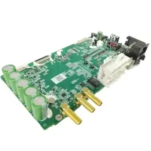
- RoHS 2 (2011/65/EU) — Restricts lead, mercury, cadmium, hexavalent chromium, PBB, PBDE, and four phthalates in electrical and electronic equipment
- REACH (EC 1907/2006) — Requires registration, evaluation, and authorization of chemical substances used in production
- IPC J-STD-006B — Specifies requirements for solder alloys used in electronic assembly
- IPC-A-610H — Defines acceptability criteria for lead-free solder joints in electronic assemblies
- China RoHS (GB/T 26572) — Mirrors EU RoHS for products sold in the Chinese market
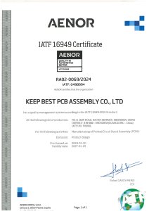
For companies manufacturing automotive electronics PCBA, the compliance landscape becomes even more stringent. The IATF 16949 standard requires documented process failure mode and effects analysis (PFMEA) for every new product introduction, with lead-free soldering parameters validated through extensive thermal cycling tests.
Quality Control Systems for Lead-Free Production
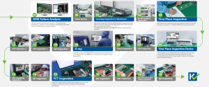
Effective quality control in lead-free PCB assembly requires a multi-layered approach that begins before the first component is placed and continues well after the final board ships. The following pillars form the backbone of a robust lead-free quality system. Each stage must be validated against IPC standards and documented in the manufacturing execution system for full traceability.
1. Incoming Material Inspection and Solder Paste Management
Solder paste is the single most critical consumable in surface mount technology (SMT) assembly for lead-free PCB assembly. Each lot of SAC305 paste undergoes viscosity testing, particle size analysis, and solder ball spread evaluation upon arrival. Storage at –10°C ± 2°C in monitored refrigerators prevents degradation, and every paste container is logged with lot number, expiry date, and exposure time to ambient conditions.
Stencils are laser-cut to the exact aperture design specified in the Gerber files, with nanocoating applied to reduce solder paste friction. This precision is especially important for fine-pitch components — 0201 and 01005 packages — where excessive paste volume leads to bridging and insufficient paste causes opens.
2.Profile Optimization for Lead-Free Alloys
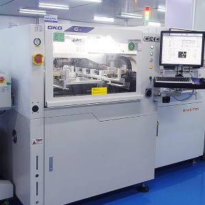
The reflow oven thermal profile is the heart of lead-free PCB assembly soldering. A standard SAC305 reflow profile consists of four zones:
- Preheat zone (25–150°C at 1–3°C/second) — Gradual temperature rise to prevent thermal shock to components and substrates
- Thermal soak zone (150–200°C, 60–120 seconds) — Activates flux, evaporates solvents, and equalizes temperatures across the board
- Reflow zone (peak 240–260°C, 30–90 seconds above liquidus) — Melts solder alloy and forms metallurgical bonds
- Cooling zone (4–6°C/second ramp-down) — Controls grain structure formation for optimal joint strength
Each profile is verified using a multi-channel data logger with thermocouples attached to the most thermally sensitive components. The data is stored in the manufacturing execution system (MES) for full traceability, allowing engineers to correlate any field failure back to the exact reflow profile used during production.
3. Automated Optical Inspection and X-Analysis
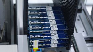
Lead-free solder joints have a duller, grainier appearance compared to the shiny surfaces of SnPb joints, making visual inspection less reliable. Modern PCBA manufacturer China facilities address this challenge with 3D automated optical inspection (AOI) systems that use structured light and multi-angle imaging to detect coplanarity defects, insufficient solder, and misalignment with sub-micron precision. In lead-free PCB assembly, these inspection systems are calibrated specifically for the matte finish of SAC305 joints, ensuring that acceptance criteria align with IPC-A-610H standards for lead-free processes.
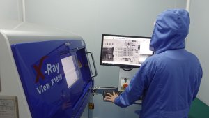
For hidden solder joints — ball grid arrays (BGA), quad flat no-leads (QFN), and through-hole connectors — X-ray inspection is mandatory. Keep Best PCBA operates 3D X-ray systems with computed tomography (CT) capability, capable of detecting voids exceeding the 25% IPC-610 limit, head-in-pillow defects, and wetting failures that are invisible to optical methods.
Certification Standards That Validate Lead-Free Processes
Certifications provide third-party validation that a manufacturer’s lead-free processes are both documented and consistently executed. Three certifications form the foundation of credible lead-free PCB assembly operations. Without these certifications, manufacturers cannot demonstrate the process discipline required by automotive, medical, and aerospace customers who depend on lead-free PCB assembly for safety-critical applications.
| Certification | Scope | Relevance to Lead-Free |
|---|---|---|
| ISO 9001:2015 | Quality management system | Requires documented procedures for process control, traceability, and corrective action |
| IATF 16949:2016 | Automotive quality management | Demands advanced product quality planning (APQP) and PPAP for lead-free soldering |
| ISO 13485:2016 | Medical device quality management | Requires risk-based validation of soldering parameters for patient safety |
As a certified PCB assembly manufacturer holding all three certifications, Keep Best PCBA maintains separate quality dossiers for each industry vertical. Automotive clients receive process flow diagrams and control plans aligned with IATF requirements, while medical device customers benefit from ISO 13485’s design transfer protocols that ensure lead-free soldering parameters are validated before clinical production begins.
Common Lead-Free Soldering Defects and Mitigation Strategies
Even with robust processes, certain defects are more prevalent in lead-free PCB assembly than in traditional SnPb soldering. Understanding their root causes enables faster troubleshooting and higher first-pass yield, ultimately reducing scrap rates and delivery lead times.
Tombstoning in Passive Components
Tombstoning occurs when one pad of a passive component wets and solidifies before the other, creating a torque that lifts the component upright. In lead-free PCB assembly, this defect is exacerbated by uneven thermal distribution and asymmetric pad design. Mitigation strategies include symmetrical pad geometry, nitrogen reflow atmosphere (reducing oxygen below 500 ppm), and optimized paste deposition volume via step stencil technology.
Voiding in BGA Solder Joints
Voiding — trapped gas or flux residue within a solder joint — is particularly problematic in lead-free BGA assemblies because SAC305’s higher surface tension traps volatiles more effectively. Controlling void rates below 25% requires vacuum-assisted reflow ovens, optimized flux chemistry with low volatile content, and pre-baking of moisture-sensitive components per JEDEC J-STD-033.
Tin Whisker Formation
Tin whiskers are crystalline structures that grow spontaneously from pure tin surfaces, potentially causing short circuits in fine-pitch applications. While SAC alloys with silver content significantly reduce whisker risk, critical applications may require conformal coating, matte tin component finishes, and periodic whisker risk assessments per JEDEC JP002.
The Role of Traceability in Lead-Free Compliance
Regulatory compliance is only as strong as the evidence supporting it. When a product is flagged for a RoHS audit or a field failure investigation, manufacturers must produce complete documentation within 72 hours. This requirement drives the implementation of MES traceability systems that link every board to its bill of materials (BOM), solder paste lot, reflow profile, inspection results, and operator identity. For lead-free PCB assembly, this traceability is not optional — it is a regulatory and contractual obligation.
Keep Best PCBA’s MES system, integrated with one-stop PCBA solution capabilities, captures data at 14 process nodes — from incoming goods through final functional testing. This granular traceability is essential for automotive electronics PCBA where IATF 16949 mandates component-level traceability for safety-critical components.
Future Trends in Lead-Free Electronics Manufacturing
The lead-free landscape continues to evolve. Several emerging trends will shape quality control practices through the remainder of this decade:
- Low-temperature SAC alternatives — Alloys such as SN100C and Bismuth-doped SAC reduce reflow temperatures to 200–210°C, lowering thermal stress on sensitive components
- AI-driven defect prediction — Machine learning models trained on AOI and X-ray data are achieving 94% accuracy in predicting solder defects before they occur
- Green chemistry fluxes — Halogen-free, water-soluble fluxes reduce environmental impact and simplify cleaning processes
- Digital twin reflow optimization — Virtual models of reflow ovens simulate thermal profiles before physical production, reducing setup time by 40%
These advancements are particularly valuable for manufacturers serving the consumer electronics PCBA market, where product lifecycles are short and new product introduction speed is a competitive differentiator. As lead-free PCB assembly continues to mature, the convergence of AI, digital twins, and green chemistry will redefine what is possible in compliant electronics manufacturing.
Conclusion
Lead-free PCB assembly is a sophisticated engineering discipline that demands rigorous process control, advanced inspection technologies, and unwavering adherence to international compliance standards. From solder paste management to AI-driven defect prediction, every step in the lead-free production chain must be validated, documented, and continuously improved.
For manufacturers seeking a reliable partner for lead-free PCB assembly, the evaluation criteria should extend beyond basic RoHS declarations. Look for contract electronics manufacturer partners who maintain ISO 9001, IATF 16949, and ISO 13485 certifications, operate 3D AOI and X-ray inspection systems, and provide MES-based traceability for every board produced.
Manufacturers who invest in comprehensive quality systems — backed by ISO 9001, IATF 16949, and ISO 13485 certifications — deliver products that meet regulatory requirements while achieving the reliability metrics demanded by automotive, medical, and industrial applications. Contact Keep Best PCBA for professional lead-free PCB assembly services backed by full compliance documentation, advanced inspection capabilities, and end-to-end traceability across all production stages.
