
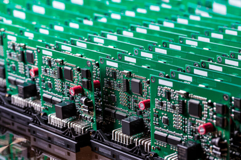
SMT (Surface Mount Technology) is the core process in PCB assembly. Quality control spans three critical stages: screen printing, component placement, and reflow soldering.

Solder Paste Printing Control
Solder paste printing accounts for over 70% of soldering defects. Stencil thickness must be selected based on component type: 0.12–0.15 mm for general components, and 0.1–0.12 mm for fine-pitch QFPs. Printing pressure, speed, and release angle must be calibrated regularly. Implementing SPI (Solder Paste Inspection) allows for real-time monitoring of printing quality to detect issues such as insufficient paste volume or misalignment.
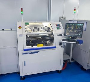
Placement Accuracy Management
The accuracy of the placement machine directly affects component positioning. Packages of 0201 and larger require placement accuracy of ±0.05 mm. Regular maintenance of the nozzles and calibration of the camera recognition system are essential preventive measures. For bottom-lead components such as BGAs and QFNs, placement pressure must be precisely controlled to prevent pad deformation.
Reflow Soldering Temperature Profile Optimization
The reflow soldering temperature profile consists of four stages: preheating, hold, reflow, and cooling. Peak temperatures are set based on solder paste type: typically 235–245°C for lead-free solder paste, with a duration of 30–60 seconds. Profile boards should be run regularly to ensure the stability of parameters across all temperature zones.

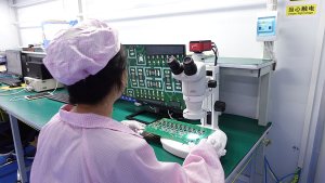
AOI (Automated Optical Inspection) Applications
AOI is deployed after reflow soldering to detect soldering defects, including insufficient solder, excess solder, bridging, component misalignment, and reversed polarity. 2D AOI is suitable for standard components, while 3D AOI measures solder joint height and is better suited for complex packages. However, AOI cannot detect BGA bottom solder joints and must be supplemented with X-ray inspection.
The Necessity of X-Ray Inspection
The hidden solder pads in packages such as BGA, QFN, and CSP are not visible. X-ray inspection can detect voids, bridging, and misalignment issues. A void rate exceeding 25% is typically deemed unacceptable, requiring adjustments to reflow parameters or stencil aperture design.

Functional Testing and Aging Validation
FCT (Functional Circuit Testing) is performed after assembly to verify electrical performance. High-temperature aging tests (72 hours at 40°C) can identify products with early failures. ICT testing requires pre-designed test points, with a coverage target typically set at 85% or higher.
Quality Data Traceability
A production data archive is established for each batch, including solder paste batch number, oven temperature profiles, and AOI inspection results. In the event of quality issues, specific processes and parameters can be traced to quickly identify the root cause.
A comprehensive SMT quality control system requires the synergy of equipment investment, process specifications, and personnel training. Selecting an ISO-certified PCB assembly factory is the fundamental guarantee for ensuring quality.
Frequently Asked Questions (FAQ)
Q1: What is the difference between SPI and AOI?
Why are both necessary? A: SPI inspects solder paste print quality (volume, offset, height) prior to reflow soldering, while AOI inspects solder joint formation (solder deficiency, bridging, offset) after reflow soldering. SPI is a preventive inspection, and AOI is a post-process verification; the two are complementary and indispensable.
Q2: Can X-ray inspection detect all BGA soldering issues?
A: X-ray can detect voids, bridging, misalignment, and missing balls, but it cannot detect micro-cracks or interface delamination. For high-reliability products (such as those in aerospace), cross-section analysis is also required for in-depth verification.
Q3: What is the difference in reflow temperatures between lead-free and leaded solder pastes?
A: Leaded solder paste (Sn63Pb37) has a peak temperature of approximately 210–220°C; lead-free solder paste (SAC305) has a peak temperature of 235–245°C, with a narrower reflow window. Lead-free processes require stricter control of the temperature profile, and it is normal for solder joints to exhibit lower gloss.
Q4: What does an ICT test coverage of 85% mean?
A: It refers to the proportion of component pins or networks covered by the test points. 100% coverage is the ideal goal, but it is limited by test point space and design density. 85% is an industry-accepted benchmark; the uncovered portions must be supplemented with verification through FCT functional testing.
Q5: Why do individual soldering defects occur in the same batch of products?
A: Possible causes include: localized blockages in solder paste printing, fluctuations in the vacuum of the placement machine nozzle, uneven temperature zones in the reflow oven, or moisture absorption by the PCB board. By tracing back through SPI/AOI data, it is usually possible to pinpoint the specific equipment and time period, allowing for targeted adjustments.