
DFM (Design for Manufacturability) serves as the critical link between PCB design and efficient production. Good DFM practices can significantly improve yield, reduce costs, and accelerate delivery.
Pad Design Specifications
The pad dimensions for surface-mount components must comply with the component datasheet. Pads that are too large can cause component misalignment (the “tombstone” effect), while pads that are too small can result in poor solder joints. For BGA devices, the ratio of pad diameter to ball diameter should be maintained between 0.8 and 1.0 to ensure reliable solder joints during reflow.

Component Spacing Requirements
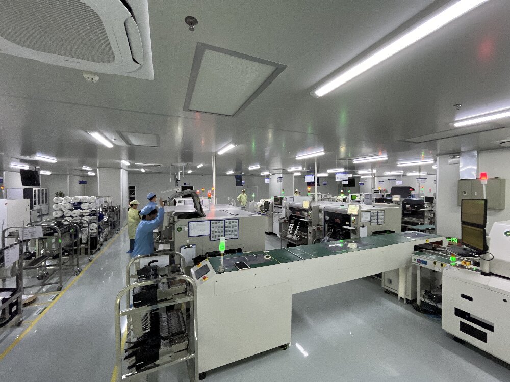
Maintain a minimum spacing of 0.2 mm between SMT components to allow for placement nozzle operation and AOI inspection. In high-density areas, balance layout density with manufacturability. Large components such as connectors and heat sinks should be placed away from fine-pitch ICs to prevent limitations on the placement machine’s precision.

Test Point Layout Strategy
At least one test point with a diameter of no less than 0.8 mm should be provided for each network. Test points should be distributed on a single side of the PCB to facilitate contact with the ICT (In-Circuit Test) probe bed. Avoid placing test points beneath components or in high-stress areas.
Thermal Management Design
High-power components require reserved copper pads and via arrays for heat dissipation. During reflow soldering, differences in heating rates between large copper pads and small pads may cause tombstoning or cold solder joints. This issue can be mitigated by using thermal isolation designs or balancing copper distribution.

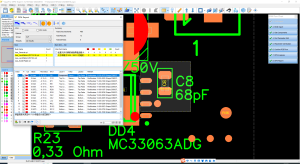
Identification and Polarity Markings
Polarized components such as diodes, electrolytic capacitors, and ICs must be clearly marked with their orientation. Silkscreen markings should avoid pads to prevent interference with soldering. It is recommended to specify polarity requirements in the BOM to reduce human error.

Panelization Design Tips
Panelization is recommended for small-sized PCBs. Add process margins, registration holes, and V-cuts or stamp holes for connections. The number of panels should balance pick-and-place machine efficiency and delamination stress; typically, 4–6 panels per sheet is appropriate.
File Preparation Checklist
Submit Gerber files, a BOM (including alternative component information), an assembly drawing, and coordinate files. Ensure that component part numbers in the BOM match those in the Gerber silkscreen to avoid placement errors.
Early DFM communication with the PCB assembly factory can prevent over 80% of manufacturing issues. It is recommended to submit a pre-review immediately after layout completion to obtain professional feedback.
Frequently Asked Questions (FAQ)
Q1: At what stage of the design process should a DFM review be conducted?
A: We recommend conducting an initial DFM review when the layout is 80% complete. At this stage, the main structure and component placement have been determined but are not yet finalized. Issues identified by the factory can still be corrected before final output, thereby avoiding revision costs.
Q2: What are some common errors in BGA pad design?
A: Common errors include: an improper ratio between pad diameter and ball diameter (should be 0.8–1.0), excessive via openings in the solder mask leading to bridging, and a lack of thermal vias resulting in excessive void rates. It is recommended to design in accordance with the IPC-7095 standard.
Q3: Why are test points necessary? What happens if there are no test points?
A: Test points serve as physical contact points for ICT and functional testing. Without test points, automated electrical testing is impossible, forcing reliance on manual visual inspection, which significantly increases the defect rate. Additionally, adding test points later requires remanufacturing the board.
Q4: What is the purpose of the process margin in panelization design?
A: The process margin is an additional area along the PCB edge used for placement machine rail clamping and optical alignment. Without a process margin, the placement machine may be unable to secure the PCB or achieve sufficient positioning accuracy. Process margins are typically 5–10 mm wide and must include alignment holes and mark points.
Q5: What problems can arise from submitting incomplete design files?
A: Missing coordinate files prevent the placement machine from identifying component locations; missing assembly drawings result in uncertainty regarding the orientation of polarized components; and discrepancies between the BOM and Gerber files lead to incorrect component placement. These issues can cause delays or even result in batch scrapping.