
The electronics manufacturing industry has undergone a fundamental shift since the European Union introduced the Restriction of Hazardous Substances (RoHS) directive in 2006. Lead-free PCB assembly is no longer an optional process refinement — it is a regulatory requirement and a competitive necessity for any PCB assembly manufacturer serving global markets. This guide examines the materials, processes, quality challenges, and compliance frameworks that define modern lead-free manufacturing.
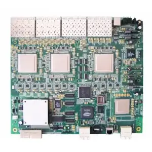
For companies producing consumer electronics, automotive systems, medical devices, and industrial equipment, understanding lead-free PCB assembly is essential to passing regulatory audits and delivering reliable products. Whether you work with a contract electronics manufacturer or operate in-house production lines, the transition from tin-lead to lead-free soldering introduces distinct technical considerations at every stage of the assembly process.
Why Lead-Free PCB Assembly Matters
Traditional tin-lead solder (63Sn/37Pb) was the industry standard for decades due to its low melting point, excellent wettability, and proven reliability. However, lead is a toxic heavy metal that poses environmental and health risks. The RoHS directive restricts the use of lead in electronic products sold in the EU, and similar regulations have been adopted in China, Japan, South Korea, and the United States.
Beyond regulatory compliance, many OEMs and brand owners now require lead-free assembly as part of their environmental, social, and governance (ESG) commitments. Major retailers and procurement platforms specify RoHS-compliant products in their supplier agreements. A manufacturer that cannot provide lead-free assembly effectively locks itself out of the most lucrative global markets.
There are limited exemptions — for example, certain medical, military, and aerospace applications may still use leaded solder under specific conditions. However, these exemptions are narrowing over time, and the vast majority of commercial electronics now require fully lead-free processes.
Lead-Free Solder Alloys and Material Selection
The core of lead-free PCB assembly is the solder alloy. Unlike tin-lead solder, which melts at 183°C, lead-free alloys have higher melting points and different wetting characteristics. Selecting the right alloy directly affects joint reliability, process windows, and defect rates.
Common Lead-Free Solder Alloys
- SAC305 (96.5% Sn / 3.0% Ag / 0.5% Cu): The most widely used lead-free alloy for SMT PCB assembly. It offers a good balance of strength, thermal fatigue resistance, and cost. Its melting range is 217–220°C.
- SAC405 (95.5% Sn / 4.0% Ag / 0.5% Cu): Higher silver content provides improved mechanical strength and thermal cycling performance, making it suitable for automotive and industrial applications.
- SN100C (Sn / 0.7% Cu / 0.05% Ni / Ge): A nickel-stabilized alloy that reduces copper dissolution in wave soldering. It produces bright, smooth joints and is popular for through-hole assembly.
- Low-temperature alloys (Sn/Bi): Used for temperature-sensitive components and flexible substrates, though brittleness concerns limit their use in high-reliability applications.
Solder paste selection also involves flux chemistry. Lead-free fluxes must be more active at higher temperatures to overcome the reduced wettability of lead-free alloys. No-clean flux systems are standard for most SMT applications, while water-soluble fluxes are used when stringent ionic cleanliness is required, such as in medical device PCB assembly.
The Lead-Free SMT Assembly Process
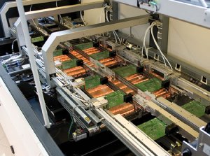
Lead-free assembly modifies several stages of the standard SMT workflow. Each adjustment compensates for the higher thermal requirements and different material behaviors of lead-free alloys.
Stencil Printing
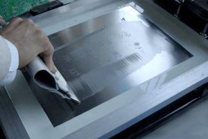
Lead-free solder paste typically has a coarser powder particle size (Type 3 or Type 4) and different rheology than tin-lead paste. Stencil aperture designs may need slight enlargement — typically 5–10% — to ensure adequate paste deposition. Nano-coated stencils reduce paste adhesion to aperture walls and improve transfer efficiency for fine-pitch components.
Component Placement
Placement accuracy requirements remain the same, but operators must verify that all components are rated for lead-free reflow temperatures. Components marked with the “e3” or higher Sn-compatibility symbol confirm lead-free terminal finishes. Mixing leaded and lead-free components on the same board creates reliability risks and should be avoided.
Reflow Soldering
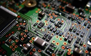
The reflow profile is the most critical adjustment in lead-free PCB assembly. Peak temperatures typically reach 245–260°C, compared to 210–220°C for tin-lead. The profile must balance complete alloy melting and intermetallic formation against thermal damage to components and substrates. Key profile zones include:
- Preheat zone: 25–150°C at 1–2°C/s to avoid thermal shock
- Soak zone: 150–200°C for 60–120 seconds to activate flux and equalize board temperatures
- Reflow zone: Peak 245–260°C with time above liquidus (TAL) of 30–90 seconds
- Cooling zone: Controlled cooling at 2–4°C/s to refine grain structure and prevent excessive intermetallic growth
For double-sided boards, the second reflow pass requires careful profile tuning to prevent component drop-off and pad de-wetting. Nitrogen atmosphere reflow is recommended for lead-free assembly to reduce oxidation and improve wetting, especially for fine-pitch and BGA components.
Quality Challenges in Lead-Free Assembly
Lead-free assembly introduces several defect modes that are less common or absent in tin-lead processes. Understanding these challenges helps manufacturers implement targeted prevention strategies.
Tin Whiskers
Tin whiskers are microscopic conductive filaments that grow spontaneously from pure tin finishes. They can bridge adjacent conductors and cause short circuits, posing a serious reliability risk in high-reliability applications. Mitigation strategies include:
- Using matte tin finishes rather than bright tin
- Adding a nickel underlayer beneath tin plating
- Applying conformal coating to isolate potential whisker growth
- Controlling plating bath chemistry and deposit stress
Voids and Solder Joint Defects
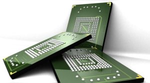
Lead-free solder is more prone to voiding — trapped gas pockets inside solder joints — particularly under BGA and QFN packages. Excessive voiding (typically >30% by area) can reduce mechanical strength and thermal conductivity. Process controls to minimize voiding include optimized flux activation, controlled soak times, and vacuum reflow systems for critical applications.
Tombstoning and Component Movement
The higher surface tension of lead-free alloys increases the risk of tombstoning, where chip components stand on end during reflow. This defect is especially prevalent with 0201 and 0402 chip components. Symmetrical pad design, balanced paste deposition, and controlled heating rates are essential preventive measures.
Inspection and Testing for Lead-Free Boards
Quality verification in lead-free assembly requires adapted inspection criteria. Lead-free solder joints have a different appearance — they are typically duller and grainier than shiny tin-lead joints, which can confuse inspectors trained on leaded processes.
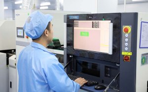
Automated Optical Inspection (AOI) systems must be recalibrated with lead-free solder joint libraries to avoid false rejects. 3D AOI adds coplanarity measurement capability, detecting insufficient solder and lifted leads that visual-only systems miss.
X-ray inspection is critical for BGA and QFN packages, where voiding and head-in-pillow defects are hidden beneath components. High-resolution 2D and 3D X-ray systems quantify void percentages and identify incomplete ball fusion.
In-Circuit Testing (ICT) and Functional Testing (FCT) verify electrical performance under operating conditions. For lead-free assemblies, test probes must account for harder solder surfaces — lead-free solder is mechanically harder than tin-lead, which can accelerate probe tip wear and require more frequent maintenance.
RoHS Compliance Documentation
Compliance with RoHS is not just about using lead-free solder — it requires comprehensive documentation throughout the supply chain. Manufacturers must maintain:
- Material declarations for all components and bare boards, confirming absence of restricted substances
- Process documentation showing that lead-free alloys and compatible materials are used consistently
- Test reports from X-ray Fluorescence (XRF) analysis verifying lead content below 1000 ppm threshold
- Compliance certificates from component suppliers confirming RoHS status of each part number
Keep Best PCBA maintains full RoHS compliance documentation as part of its ISO 9001 quality management system, providing customers with audit-ready compliance packages for every production order. This is particularly important for customers shipping to the EU, where CE marking requires RoHS conformity.
Choosing a Lead-Free PCB Assembly Partner
Not all manufacturers handle lead-free assembly with the same level of expertise. When evaluating a partner for lead-free PCB assembly, consider these critical factors:
- Process maturity: How long has the manufacturer been running lead-free lines? Look for at least 5+ years of lead-free production experience with documented process parameters.
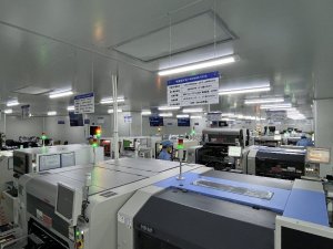
- Equipment capability: Nitrogen-capable reflow ovens, lead-free-rated wave soldering equipment, and calibrated AOI/X-ray systems are minimum requirements.
- Component sourcing: The partner should have established supply chains for RoHS-compliant components and verify lead-free status at incoming inspection.
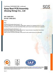
- Certification alignment: ISO 9001, ISO 13485, and IATF 16949 certifications demonstrate a quality management system capable of controlling lead-free processes to industry standards.
- Technical support: A capable manufacturer provides DFM feedback on lead-free design considerations, including component compatibility, thermal management, and pad design optimization.
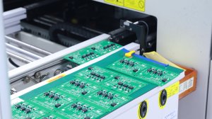
Keep Best PCBA operates fully lead-free production lines across its Shenzhen, Jiangmen, and Thailand facilities, backed by electronic manufacturing services that cover everything from one-stop PCBA solution design support to mass production. With ISO 9001, ISO 13485, and IATF 16949 certifications, the company serves automotive, medical, consumer electronics, and industrial clients who require compliant, reliable assemblies.
Conclusion
Lead-free PCB assembly is a non-negotiable requirement for electronics products entering global markets. The transition from tin-lead to lead-free alloys introduces higher process temperatures, different defect modes, and stringent compliance documentation requirements. Success depends on proper alloy selection, optimized reflow profiles, robust inspection protocols, and a thorough understanding of lead-free material behavior.
By partnering with an experienced manufacturer that maintains certified lead-free processes, companies can navigate RoHS compliance confidently and deliver products that meet both regulatory standards and customer expectations for reliability. Contact Keep Best PCBA for professional lead-free assembly services, from prototyping through mass production, with full RoHS compliance documentation and quality assurance at every stage.
