
SMT PCB Assembly Process: A Complete Step-by-Step Guide for 2026
Surface mount technology has become the dominant method for producing electronic circuit boards worldwide. Understanding the SMT PCB assembly process is essential for engineers, procurement managers, and product developers who need predictable quality, competitive pricing, and fast turnaround from their manufacturing partners. Whether you are building a prototype run or scaling to millions of units, each step in the process directly influences your final product reliability and cost.
This guide walks through every stage of SMT PCB assembly, from initial design review through final inspection, with practical tips that help you avoid common defects and optimize your production yield. Along the way, we explain where DFM analysis fits, how PCB components procurement impacts your schedule, and when through-hole PCB assembly should complement your surface mount layout.
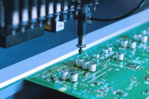
What Is SMT PCB Assembly and Why It Dominates Modern Manufacturing
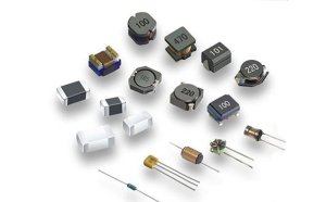
SMT PCB assembly is the process of soldering electronic components directly onto the surface of a printed circuit board, rather than inserting leads through drilled holes. Components mounted this way — resistors, capacitors, integrated circuits, and connectors — are smaller, lighter, and pack more functionality per unit of board area than their through-hole equivalents.
Several factors explain why SMT PCB assembly accounts for over 90 percent of all board production today:
- Higher density: 0201 and 01005 passive components enable designs that would be impossible with through-hole technology.
- Faster assembly speed: Modern pick-and-place machines mount up to 150,000 components per hour, dramatically reducing cycle time.
- Lower per-unit cost: Smaller components, automated placement, and reduced board area all contribute to significant cost savings at volume.
- Better electrical performance: Shorter lead lengths reduce parasitic inductance and capacitance, improving signal integrity at high frequencies.
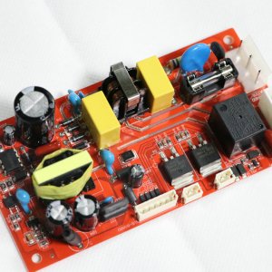
That said, not every component fits the SMT paradigm. Power devices, large connectors, and mechanical parts often still require through-hole PCB assembly for strength, thermal dissipation, or regulatory compliance. A skilled PCB assembly manufacturer will mix both technologies on the same board when the design demands it.

Step 1 — Design for Manufacturing (DFM) Review
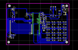
Before any physical assembly begins, your design files must pass a DFM analysis. This review checks your Gerber data, BOM, and placement files against the manufacturer’s capability matrix to catch issues that would cause defects or delays on the production line.
A thorough DFM review typically covers these areas:
- Footprint accuracy: Pad sizes must match the component’s data sheet. Oversized pads waste solder paste; undersized pads cause weak joints or tombstoning.
- Component spacing: Minimum clearances between parts prevent shadowing during reflow and allow room for inspection probes.
- Panelization strategy: Breaking a single board design into a multi-up panel reduces handling time but requires correct fiducial placement and breakout tab design.
- Thermal relief: Large copper pours connected to small pads need thermal reliefs so the pad reaches reflow temperature without stealing heat from the plane.
When DFM problems are found, the manufacturer returns a report with specific recommendations. Fixing these issues before production begins is far cheaper than discovering them after a failed first-article run. A reliable one-stop PCBA solution provider will include this review as a standard step rather than an optional add-on.
Common DFM Mistakes That Delay Production
The most frequent errors include:
- Placing fiducial marks too close to board edges, where they get trimmed during depanelization.
- Specifying components that are obsolete or on allocation without confirming availability during PCB components procurement.
- Using non-standard package sizes that the manufacturer’s pick-and-place machines cannot handle without custom nozzles.
- Designing symmetrical footprints for polarized parts (diodes, electrolytic capacitors), which leads to reversed placement.
Addressing these before you commit to production keeps your schedule intact and your yield high.
Step 2 — Solder Paste Stencil Design and Printing
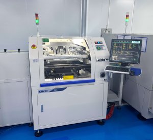
Solder paste printing is the single most critical step in SMT PCB assembly. Studies consistently show that 60 to 70 percent of all solder joint defects originate at the printing stage. The stencil — a thin metal sheet with laser-cut or electroformed apertures — controls how much solder paste deposits on each pad.
Key stencil design parameters include:
- Stencil thickness: 0.12 mm suits fine-pitch components (0.4 mm QFP, 0.5 mm BGA). 0.15 mm works better when the board mixes fine-pitch ICs with larger passives and power components.
- Aperture area ratio: The ratio of aperture open area to sidewall area should exceed 0.66 for laser-cut stencils. Below this threshold, paste release suffers and volumes become inconsistent.
- Step-down regions: When a board combines large connectors with 0.4 mm pitch chips, a stepped stencil reduces paste volume locally without sacrificing deposit height elsewhere.
- Nano-coating: A hydrophobic surface treatment on the stencil improves paste release for ultra-fine-pitch designs and extends cleaning intervals.
After printing, solder paste inspection (SPI) scans every deposit for volume, height, and alignment. SPI data feeds directly into process control dashboards, letting the operator adjust printing pressure, speed, or snap-off distance before defects accumulate.
Printing Process Parameters That Affect Yield
Four variables dominate print quality:
- Squeegee pressure: Too low and the paste fails to fill apertures completely. Too high and it smears across the stencil surface, creating bridging between adjacent pads.
- Print speed: Faster speeds reduce fill time, which can starve fine-pitch apertures. Slower speeds improve fill but increase cycle time.
- Snap-off distance: The gap between stencil and board during separation controls how cleanly the paste transfers. A larger snap-off helps release but can stretch tall deposits.
- Paste viscosity and metal content: Type 4 paste (20-38 µm particle size) suits 0.4 mm pitch. Type 5 (10-20 µm) is required for 0.3 mm pitch and below. Metal content above 88 percent by weight improves joint strength but reduces paste flow.
Controlling these variables with real-time SPI feedback keeps your first-pass yield above 98 percent on most board designs.
Step 3 — High-Speed Component Placement
Once solder paste sits on the pads, the pick-and-place machine mounts every component according to the centroid file derived from your CAD data. Modern placement equipment operates at extraordinary speed and precision:
- Chip shooters handle passive components (0201, 0402, 0603) at speeds above 100,000 CPH with placement accuracy of ±25 µm.
- Flexible placers handle ICs, BGAs, and odd-form components at 20,000-40,000 CPH with accuracy down to ±10 µm.
- Multi-gantry systems split the placement task across independent heads, reducing cycle time on boards with hundreds of unique part numbers.
Placement accuracy depends on several upstream inputs:
- Feeder setup: RFID-tagged reels verify that the correct part is loaded in the correct feeder slot, eliminating manual verification errors.
- Fiducial alignment: Global fiducials on the panel and local fiducials near fine-pitch components correct for board stretch, rotation, and tooling offsets.
- Vision recognition: Upward-looking cameras inspect component polarity marks, orientation, and co-planarity before placement, rejecting defective parts before they reach the board.
When placement errors occur — a shifted BGA or a reversed diode — they are expensive to fix after reflow. Catching them at the placement stage through vision verification and proper fiducial use is far more efficient.
Step 4 — Reflow Soldering Profile Optimization
Reflow soldering melts the solder paste deposits, permanently bonding each component to its pads. The thermal profile — the sequence of temperature zones the board passes through in the reflow oven — must be tuned to the paste chemistry, component mix, and board thickness.
A standard lead-free reflow profile includes four phases:
- Preheat zone (25-150 °C): Gradual temperature rise activates flux solvents and evaporates moisture from the paste. Too fast and volatile components pop, scattering solder balls across the board.
- Thermal soak zone (150-200 °C): Flux activates fully and cleans oxide layers from pads and component terminations. This zone also equalizes temperature across the board, preventing thermal gradients that cause tombstoning on small passives.
- Peak zone (230-250 °C): Solder melts and wets both the pad and the component termination. Peak temperature must exceed the solder’s liquidus point by 15-25 °C but stay below component damage thresholds. Time above liquidus (TAL) should be 30-90 seconds.
- Cooling zone (200-60 °C): Controlled cooling forms a fine-grained solder joint structure. Cooling rates between 1-4 °C per second produce strong, reliable joints. Faster cooling creates brittle microstructures; slower cooling allows intermetallic growth that weakens the joint.
Each board design needs its own profile. Dense boards with large BGAs require longer soak times to bring the BGA center balls to melting temperature. Thin flex circuits need shorter profiles to prevent adhesive degradation. Your manufacturer should profile every new product using thermocouples attached to critical component locations and review the profile data before starting production.
Reflow Defects and How to Prevent Them
Common reflow-related defects include:
- Tombstoning: Small passives (0201, 0402) lift on one end due to uneven heating. Fix: optimize soak zone for thermal balance, and ensure symmetrical pad sizes in your design.
- Solder balls: Tiny spheres scatter around pads when paste spatters during preheat. Fix: reduce preheat ramp rate and ensure paste is stored at proper humidity.
- Voiding in BGA joints: Gas trapped in large BGA pads reduces mechanical strength. Fix: extend TAL, use vacuum reflow for critical applications, and select low-voiding paste formulations.
- Graping: Partially melted paste leaves grainy, insufficient joints. Fix: verify peak temperature reaches the recommended level and that paste has not expired.
Step 5 — Post-Soldering Inspection and Testing
After reflow, every board undergoes multiple inspection stages to verify joint quality and functional correctness:
- Automated optical inspection (AOI): Cameras scan solder joints for shape, volume, and alignment. AI-powered AOI systems at Keep Best PCBA achieve false-positive rates below 0.5 percent, reducing manual review time while catching defects traditional rule-based systems miss.
- X-ray inspection: Hidden joints under BGAs, QFNs, and CSPs cannot be seen visually. 3D X-ray systems reconstruct cross-sectional images, revealing voids, shorts, and missing balls inside the package.
- In-circuit test (ICT): A bed-of-nails fixture probes critical nets to verify component values, connectivity, and basic functionality. ICT catches solder opens, wrong component values, and assembly errors that visual inspection cannot detect.
- Functional circuit test (FCT): The board is powered and exercised through its full operating sequence, confirming that it performs its intended function before shipping.
The combination of AOI, X-ray, ICT, and FCT provides overlapping coverage that drives cumulative defect detection rates above 99.9 percent for mature SMT PCB assembly processes. A manufacturer with ISO 9001, ISO 13485, and IATF 16949 certifications — like Keep Best PCBA — maintains documented inspection procedures and statistical process controls that keep these detection rates consistent across every production run.
When to Combine SMT with Through-Hole PCB Assembly
Many products require both technologies on the same board. Understanding when through-hole PCB assembly is necessary helps you design boards that your manufacturer can assemble efficiently:
- High-power components: Transformers, large inductors, and power modules need the mechanical strength of through-hole leads to withstand vibration and thermal cycling.
- Edge connectors: D-sub, USB, and Ethernet connectors with frequent mating cycles are more durable when their pins penetrate the board and are soldered on both sides.
- High-voltage isolation: Components operating above 500 V benefit from the greater creepage and clearance distances that through-hole mounting provides.
- Mechanical switches and buttons: User-interface components subject to repeated physical force need through-hole mounting to resist pull-out and breakage.
Mixed-technology assembly typically follows a specific sequence: SMT components are placed and reflowed first, then the board moves to a manual or automated station for through-hole PCB assembly. Wave soldering or selective soldering machines handle the through-hole joints without disturbing the already-reflowed surface mount parts. Proper process sequencing and fixture design prevent re-melting of SMT joints during the second soldering pass.
For complex mixed-technology boards, choosing a manufacturer with both SMT and through-hole capability on the same production line eliminates the need to ship partially assembled boards between facilities. Keep Best PCBA’s integrated workflow handles mixed technology in a single facility, reducing lead time and logistics risk.
Conclusion
Each stage of the SMT PCB assembly process — from DFM review through stencil printing, placement, reflow, and inspection — contributes to your product’s final quality and reliability. Skipping or shortcutting any step creates defects that compound downstream, increasing rework cost and delivery delays.
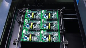
Working with an experienced manufacturer who applies rigorous process control at every stage is the most reliable path to high-yield production. From initial DFM feedback through final functional testing, a well-executed SMT PCB assembly process delivers boards that meet your specifications on the first run.
Contact Keep Best PCBA for professional SMT PCB assembly services backed by ISO-certified quality systems, AI-driven inspection, and integrated through-hole capability. Our engineering team reviews your design before production begins, ensuring that every board you receive works exactly as intended.