
What are the requirements for PCBs in PCBA manufacturing?
PCBA surface-mount assembly is the process of mounting electronic components onto a PCB using surface-mount technology. It is one of the primary processes in modern electronics manufacturing and is characterized by a high degree of automation, small component sizes, and high assembly density. PCBA assembly imposes very strict requirements on PCBs, covering multiple aspects such as soldering quality, component layout, anti-static measures, heat resistance, and via size consistency. Meeting these key requirements not only improves manufacturing quality but also effectively reduces the rework rate, ensuring product reliability and performance.
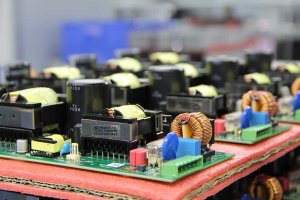
PCBA surface-mount assembly comprises six core stages
The basic process of PCBA surface-mount assembly includes the following six stages. PCB inspection involves a visual inspection of the PCB prior to assembly to ensure there is no damage or contamination. Solder paste printing uses a stencil to precisely apply solder paste to the pads on the PCB; the quality of the solder paste directly affects the soldering results. Component placement uses high-speed placement machines to position surface-mount components onto their corresponding pads. Reflow soldering secures components to the PCB through precise temperature control; the temperature profile must be carefully managed to ensure soldering quality. AOI inspection uses automated optical inspection technology to verify solder joint quality, component placement, and orientation. Functional testing evaluates the electrical performance of the assembled PCBA to ensure the product functions properly. Each stage requires the PCB to meet specific standards to ensure reliable soldering and optimal component layout.
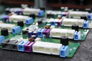
Pad Design Determines Soldering Quality and Reliability
Pads on the PCB must be precisely designed according to the component’s size and package type. If a pad is too large or too small, it may lead to unstable solder joints, resulting in cold solder joints or cold soldering, which affects the product’s electrical performance. According to the IPC-2221 standard, pad dimensions should match the size of the component leads to ensure sufficient contact in the soldering area. Proper pad design is the foundation for forming reliable solder joints and directly impacts the product’s long-term stability.
Surface Treatment Processes Affect Solder Wettability
The surface treatment of a PCB determines its solder wettability. Common surface treatment processes include HASL (Hot Air Leveling), OSP (Organic Solderable Phosphate), and ENIG (Electroless Nickel-Gold). Each surface treatment has a different impact on soldering results; typically, an ENIG surface provides superior solderability and oxidation resistance, making it suitable for high-precision, high-demand electronic products. Selecting the appropriate surface treatment process can significantly improve solder wetting and solder joint reliability.
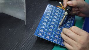
Flatness Control Prevents Soldering Defects
The flatness of a PCB directly affects soldering quality. If a PCB is bent or warped, components cannot align precisely with the pads during soldering, leading to soldering defects. The IPC-A-610 standard specifies that PCB warpage should not exceed 0.75%. Strict control of PCB flatness ensures precise alignment between components and pads during the SMT process, reducing the occurrence of issues such as cold solder joints and misalignment.
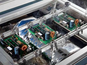
Component Placement and Routing Must Be Reasonably Planned
The rationality of component placement and PCB routing design is crucial for SMT manufacturing. Appropriate spacing should be maintained between components to avoid mutual interference, especially in high-density circuit designs. If spacing is too small, it not only increases the difficulty of placement but may also lead to solder shorts or thermal issues. It is recommended to follow the spacing requirements in the IPC-7351 standard to ensure process feasibility and product reliability. For critical electronic components such as crystal oscillators and processors, the layout should comply with thermal management and electrical performance requirements to avoid interference from other components or the effects of heat conduction. Typically, crystal oscillators should be placed as close as possible to the relevant circuits while maintaining a certain distance from high-heat-generating components. PCB routing affects signal transmission quality. Especially in high-speed circuits, signal traces should be kept as short and straight as possible to avoid signal delays or interference caused by excessively long traces. For differential signals and power lines, appropriate routing techniques—such as running traces in parallel or ensuring equal trace lengths—should be used to ensure signal integrity.

Electrostatic Discharge (ESD) Protection for Sensitive Components
ESD protection is a critical aspect of PCBA manufacturing, as electrostatic discharge can damage sensitive electronic components. Anti-static measures should be fully considered during PCB design, including the use of materials or coatings with anti-static properties, particularly in high-density and high-frequency circuits. In PCB layout design, ground planes should be arranged appropriately to ensure that static electricity in the circuit can be effectively dissipated. Grounding design not only helps eliminate static electricity but also enhances the circuit’s immunity to interference, ensuring product safety during manufacturing and use.

Material Heat Resistance Must Match Processing Temperatures
During the PCBA surface-mount assembly process, PCBs undergo repeated heating, particularly during the reflow soldering stage, where temperatures can reach 250°C; therefore, PCBs must be able to withstand high temperatures. The glass transition temperature (TG) of a PCB material determines the maximum temperature it can withstand; typically, the TG value should range between 130°C and 170°C. For electronic products operating in high-temperature environments, such as automotive electronics, PCB materials require a higher TG value to ensure long-term reliability. During SMT processing of multilayer PCBs, the bond strength between layers must be ensured to prevent delamination during high-temperature soldering; the quality of the laminate material directly affects the PCB’s mechanical and electrical performance.
Via Diameter Consistency Ensures Assembly Precision
Through-holes and pads on PCBs must meet very high consistency requirements, particularly during via plating and soldering processes. Any inconsistency in hole diameter or insufficient via filling will affect the electrical connection of components and assembly accuracy. In PCB manufacturing, via diameter tolerances must be strictly controlled; the typically allowed tolerance range is ±0.05 mm. If the hole diameter error is too large, it may result in difficulty inserting components or compromise soldering quality. The spacing between pads must precisely match the dimensions of the component leads to ensure stable placement during the SMT process and prevent misalignment or warping.
Conclusion
PCBA surface-mount assembly imposes comprehensive and stringent requirements on PCB soldering quality, layout and routing, electrostatic discharge (ESD) protection, heat resistance, and via diameter consistency. By optimizing pad design, selecting appropriate surface treatment processes, controlling board flatness, planning component layout rationally, implementing ESD protection measures, using high-heat-resistant materials, and ensuring via diameter accuracy, it is possible to significantly improve manufacturing quality, effectively reduce rework rates, and ensure product reliability and market competitiveness.