

Wearable electronics represent one of the most demanding categories of PCB assembly. Smartwatches, fitness trackers, true wireless earbuds, and health monitoring patches combine extreme miniaturization, wireless connectivity, battery management, and consumer-grade reliability expectations in form factors measured in millimeters. The manufacturing challenges these products create require specialized capabilities that go well beyond standard SMT assembly.
This article examines the specific assembly challenges of wearable electronics and the manufacturing strategies that successful wearable brands use to meet them.
The Miniaturization Challenge
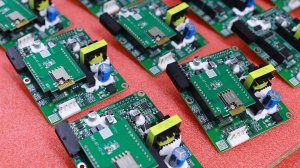
Wearable devices pack significant functionality into extremely small volumes. A typical smartwatch PCB may measure 25mm by 35mm and host a microprocessor, wireless chipset, memory, power management, sensors, and passive components. This density requires assembly capabilities at the extreme end of current technology.
Component sizes on wearable boards routinely include 0201 and 01005 passives, components so small they are barely visible to the naked eye. A 01005 resistor measures 0.4mm by 0.2mm, smaller than a grain of sand. Placing these components requires placement machines with ultra-high precision, specialized nozzles, and vision systems capable of resolving and measuring components at the limits of optical resolution.
Solder paste printing for 01005 components pushes stencil technology to its limits. The aperture for a 01005 pad may be only 0.2mm wide, requiring a stencil thickness of 0.08mm or thinner to achieve the area ratio needed for complete paste release. At these dimensions, paste particle size becomes critical; Type 4 or Type 5 paste with smaller particles is necessary for reliable printing through ultra-fine apertures.
The cumulative effect of these miniaturization challenges is that wearable assembly requires a manufacturing environment calibrated for precision at every process step. Squeegee pressure, squeegee speed, squeegee angle, stencil separation speed, ambient temperature, and humidity all must be controlled within tighter tolerances than standard SMT assembly. A manufacturing partner without specialized fine-pitch capability cannot reliably produce wearable electronics.

Package-on-Package and Embedded Components
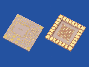
To achieve the density required for wearables, designers increasingly use package-on-package stacking and embedded component technology. PoP stacking places a memory package directly on top of a processor package, reducing the combined footprint by the area of the memory package. This technology is nearly universal in TWS earbuds and increasingly common in smartwatches.
Embedded component technology takes miniaturization further by burying passive components within the PCB layers during fabrication. Resistors and capacitors formed from internal copper planes and dielectric materials eliminate the surface area these components would otherwise consume. While embedded components add fabrication complexity and cost, the space savings can be decisive in form-factor-constrained designs.
Both technologies require assembly partners with specific experience. PoP assembly demands flux dispensing capabilities for the inter-package balls, precise stacking alignment, and reflow profiles optimized for the thermal mass of stacked packages. Embedded component technology requires coordination between the board fabricator and the assembly partner to ensure that the embedded components are correctly specified and that the assembly process accommodates any thermal or mechanical constraints they impose.
Flexible and Rigid-Flex Substrates in Wearables
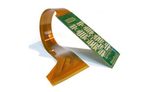
Many wearable products use flexible or rigid-flex PCB substrates to fit within curved or irregular housings. TWS earbuds typically use small rigid-flex assemblies that fold into the earbud housing. Smartwatches use flex circuits to connect the main board to the display, battery, and sensors distributed around the watch case. Health monitoring patches may use entirely flexible substrates that conform to body contours.
Flex substrate assembly introduces handling challenges that rigid board assembly does not face. The thin polyimide substrates are easily damaged by handling, requiring specialized carrier pallets for printing, placement, and reflow. The substrates expand and contract more than FR-4 during thermal cycling, requiring modified process parameters and tooling that accommodates dimensional movement.
Conformal coating or encapsulation is often required for wearable assemblies to protect against moisture, sweat, and mechanical stress. The coating material must be compatible with the flex substrate and must not crack or delaminate during repeated flexing. Selective coating application must avoid coating on areas that require flexibility, as coating stiffens the substrate and can cause cracking at flex points.
Reliability Under Consumer Use Conditions
Wearable devices face reliability challenges that most consumer electronics do not encounter. They are worn on the body, exposed to sweat, skin oils, and cosmetic products. They experience mechanical shock from impacts and continuous vibration from movement. They undergo temperature cycling from body heat, ambient temperature changes, and charging cycles. And consumers expect them to survive daily use for two to three years without failure.
Sweat is particularly aggressive to electronic assemblies. The salt content creates ionic contamination that can cause electrochemical migration, dendrite growth, and eventual short circuits. Conformal coating or encapsulation is essential for any wearable with exposed circuitry near the skin. The coating must provide complete coverage with no pinholes or thin spots where moisture can penetrate.
Mechanical reliability requires attention to component selection and placement. Heavy components should be avoided on flex areas. BGA packages may require underfill to prevent solder joint fatigue under mechanical stress. Connector selection should prioritize devices rated for the expected mating cycles over the product lifetime. And the assembly should be designed so that the most likely failure points, such as battery connections and sensor interfaces, are accessible for repair.
Accelerated life testing is essential for wearable products. Temperature cycling between -20 and 70 degrees Celsius for hundreds of cycles verifies solder joint reliability. Mechanical shock and vibration testing simulates drop and wear conditions. IP rating testing verifies moisture and dust ingress protection. These tests should be performed on production-representative assemblies, not just prototypes, to ensure that the production process produces assemblies that meet reliability targets.

Volume Production and Cost Management
Successful wearable products typically ship in high volumes, from hundreds of thousands to tens of millions of units. At these volumes, small per-unit cost differences have large total impact. A one-dollar cost reduction per board translates to hundreds of thousands or millions of dollars in savings over the product lifecycle.
Cost management for wearable assembly starts with design. Component count should be minimized through integration, using multi-function ICs instead of separate devices. Layer count should be optimized; adding layers increases cost but may enable smaller board area. Panel utilization should be maximized; small boards arranged efficiently on a standard panel can significantly reduce per-board fabrication cost.
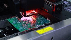
Assembly process efficiency at volume requires stable, repeatable processes with high first-pass yield. A 95 percent first-pass yield means 5 percent of boards require rework, adding labor cost and reducing throughput. At wearable volumes, even small yield improvements have significant cost impact. Process optimization during pilot production, before volume ramp-up, is essential for achieving the yield targets that make the product economically viable.
Test strategy for high-volume wearable production must balance test coverage against cycle time. Automated optical inspection and X-ray inspection provide fast, comprehensive defect detection. In-circuit testing verifies component functionality but requires test points that consume board area. Functional testing exercises the complete device but may have longer cycle times. The optimal test strategy combines these methods to achieve necessary coverage while maintaining production throughput.
Producing wearable electronics at scale requires a PCB assembly manufacturer with ultra-fine-pitch capability, flex substrate experience, and high-volume production infrastructure. The right PCBA partner brings the equipment, process engineering, and quality systems needed to produce reliable wearable devices at the volumes and cost points the market demands.
