
PCB Assembly Process Flow: From Solder Paste to Final Testing Step by Step
Understanding the PCB assembly process flow helps engineers design for manufacturability, buyers evaluate supplier capabilities, and project managers set realistic production timelines. While every assembly house tailors its workflow to specific equipment and product mix, the fundamental process steps are universal across the industry.
This article walks through each stage of the assembly process, explaining what happens, why it matters, and how quality is verified at each step. Follow along to understand how a bare circuit board becomes a fully functional electronic assembly.
Stage 1: Incoming Material Inspection and Preparation
Quality assembly begins before any solder paste touches a board. Incoming inspection verifies that all materials entering production meet specifications. Bare PCBs are inspected for dimensional accuracy, surface finish quality, solder mask registration, and physical damage from shipping. Even minor board defects cause assembly problems downstream, so catching them at incoming inspection is far cheaper than discovering them after components are soldered.
Components undergo incoming verification including quantity counts, part number confirmation against the BOM, date code and lot code recording for traceability, and visual inspection for physical damage or corrosion. Components identified as moisture-sensitive per J-STD-033 are checked for exposure history. Those exceeding exposure limits are baked according to manufacturer specifications before being released to production.
For manufacturers following advanced quality planning processes, first-article inspection of new component deliveries adds an additional layer of verification. A sample of each new lot is measured dimensionally and tested for solderability before the full quantity enters production inventory. This step prevents a common and costly scenario: discovering that a component supplier made an undocumented change only after assembly defects appear.
Stage 2: Solder Paste Printing
Solder paste printing is where the assembly process begins in earnest. A stencil, typically laser-cut stainless steel, is aligned over the bare PCB using fiducial marks for precise registration. Solder paste is applied to the stencil surface and a squeegee blade sweeps across, forcing paste through the stencil apertures onto the corresponding PCB pads.
The variables that determine print quality include squeegee pressure, speed, and angle, stencil separation speed after printing, paste temperature and viscosity, stencil cleaning frequency, and environmental conditions including temperature and humidity.
Print quality is verified by solder paste inspection equipment immediately after printing. SPI systems measure paste deposit volume, height, area, and positional accuracy for every deposit on every board. Statistical data from SPI feeds back into process control, with automatic alerts when print quality trends toward control limits. If a board fails SPI criteria, it is cleaned and reprinted rather than proceeding through the line.
Under-stencil cleaning is performed at regular intervals, typically every five to ten prints depending on paste type and aperture density. Automated stencil cleaning systems use lint-free wipes and cleaning solvent to remove paste residue from the underside of the stencil, preventing the gradual smearing that degrades print quality over extended runs.
Stage 3: Solder Paste Inspection
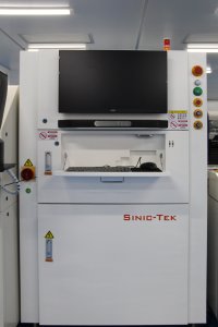
SPI deserves its own stage designation because of its critical role as a process gate. The SPI system makes a binary decision for every board: proceed to component placement, or return for cleaning and reprinting. This single decision point prevents the majority of soldering defects from propagating downstream where they become progressively more expensive to address.
Modern SPI systems generate rich data beyond pass/fail decisions. Paste volume trend charts identify gradual squeegee wear before it affects print quality. Deposit offset measurements detect fixturing issues that cause progressive misalignment. Area ratio calculations verify that the stencil design is appropriate for the paste type and aperture geometries. Engineering teams that actively analyze SPI data catch process issues earlier and achieve higher sustained yields than those using SPI solely as a pass/fail gate.
Stage 4: Component Placement
Component placement is the most visually dramatic stage of SMT assembly. High-speed placement machines, often called pick-and-place or chip shooters, place components at rates measured in tens of thousands per hour. The machines use vacuum nozzles to pick components from feeders, verify component orientation and dimensions with onboard vision systems, and place them onto solder paste deposits with micron-level precision.
Placement programs are generated from CAD data, translating component X-Y coordinates, rotation angles, and package types into machine instructions. Program optimization balances placement speed against accuracy requirements. Fine-pitch and BGA components are typically placed last, after the smaller passives, to reduce the distance they travel on the conveyor and the associated vibration.
Component feeders are the most failure-prone element of the placement system. Tape-and-reel feeders must advance reliably without damaging delicate paper or plastic carrier tapes. Tube feeders must present components consistently and detect empty tubes before they cause placement gaps. Tray feeders must index precisely to present components at consistent pickup positions.
Intelligent feeder systems with integral component verification have significantly reduced feeder-related defects. RFID tags on component reels are read when the feeder is loaded, with the system confirming that the correct part number is loaded in the correct feeder position. Any mismatch triggers an alarm before production begins. This verification step alone has been shown to eliminate the most common cause of wrong-component defects in SMT assembly.
Stage 5: Pre-Reflow Inspection
Some manufacturers include a pre-reflow automated optical inspection step after placement but before soldering. This inspection verifies that all components are present, correctly oriented, and positioned on their pads. Pre-reflow inspection catches placement errors while they are still easy to correct: the components are held in place by tacky paste, so a misplaced component can simply be removed and re-placed without desoldering.
Pre-reflow inspection is particularly valuable for high-mix production where changeover frequency increases the risk of setup errors, assemblies with high component counts where the probability of a placement error increases with component quantity, and first-article builds where the placement program is being validated for the first time.
Stage 6: Reflow Soldering
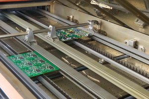
The reflow oven is where the physical transformation from loose components to soldered assembly occurs. The populated board enters the oven on a conveyor and passes through multiple heating zones, each precisely controlled to achieve the target temperature profile.
The reflow profile has four distinct phases. Preheat raises the board from ambient to approximately 150 degrees Celsius at a controlled rate to avoid thermal shock. Thermal soak holds the temperature steady, allowing all components and board areas to reach uniform temperature. Reflow raises the temperature above the solder melting point, typically peaking at 235 to 250 degrees Celsius for lead-free SAC alloys. Cooling brings the assembly back to near-ambient temperature at a controlled rate, allowing solder joints to solidify with proper grain structure.
Profile development for each product involves attaching thermocouples to representative locations on a test board and running it through the oven. Multiple profiles may need to be tested to find the optimum balance of peak temperature, time above liquidus, and cooling rate. The profile is validated by inspecting solder joint quality on the profiled board and may be adjusted based on inspection results.
Stage 7: Post-Reflow Inspection
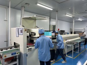
After reflow, the assembly undergoes automated optical inspection to verify solder joint quality. AOI systems compare every solder joint against programmed acceptance criteria and flag defects including solder bridges, insufficient or excess solder, component misalignment, tombstoning, and missing or incorrect components.
The AOI programming process defines what the system considers acceptable. This programming is based on IPC-A-610 criteria appropriate to the product class. Well-programmed AOI systems achieve high defect detection rates while minimizing false calls that consume operator review time. Programming quality is the single largest factor in AOI effectiveness; the same equipment can produce excellent or mediocre results depending on the programming investment.
For BGA, QFN, and other hidden-joint components, X-ray inspection supplements AOI. X-ray systems peer through component bodies to inspect solder balls and thermal pad connections that are invisible to optical systems. Voiding analysis identifies gas pockets within solder joints that weaken mechanical and thermal performance. IPC-7095 provides voiding acceptance criteria for BGA assemblies.
Stage 8: Through-Hole and Secondary Assembly
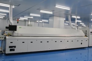
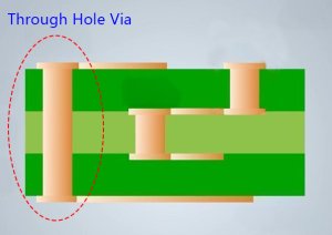
If the assembly includes through-hole components that cannot be reflow-soldered due to temperature sensitivity, they are placed and soldered in a separate process. Wave soldering passes the board over a flowing wave of molten solder, soldering all through-hole leads simultaneously. Selective soldering uses a programmable nozzle to solder individual through-hole joints with precise control over solder volume and dwell time.
Post-soldering operations may include press-fit connector installation, heatsink attachment using thermal interface materials, conformal coating application for environmental protection, depanelization of individual boards from the assembly panel, and final cleaning if required by the product specification.
Stage 9: Functional Testing
The final verification step is functional testing, confirming that the assembled board operates according to its design specifications. Test coverage and methodology vary by product complexity and application criticality. In-circuit testing verifies individual component values and basic connections. Flying probe testing provides similar capability without dedicated fixturing, suitable for lower volumes. Functional testing exercises the board as a system, verifying that it performs its intended functions. Boundary scan testing uses JTAG interfaces to test interconnects between compliant devices.
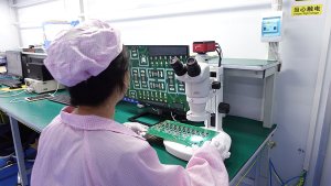
A well-designed test strategy balances test coverage against cost and cycle time. Over-testing adds unnecessary cost. Under-testing allows defects to escape to customers. The right strategy is informed by the product’s risk profile, volume, and end application requirements.
Understanding this PCB assembly process flow enables better design decisions, more accurate project planning, and more productive relationships with manufacturing partners. When you understand what happens at each process stage and why each quality gate matters, you can design boards that flow smoothly through the process with minimal rework. A full-service PCBA manufacturer should be able to walk you through their specific implementation of each stage and explain how they optimize it for your particular product type.