
Can Boundary Scan JTAG Really Replace Functional Test in PCB Assembly?
Modern PCB assemblies are denser than ever. Components shrink, ball-grid arrays hide solder joints beneath the package, and test-point access shrinks with every design cycle. Engineers face a familiar dilemma: how do you verify a board when physical probe access is nearly impossible? Boundary scan JTAG, standardized under IEEE 1149.1, has emerged as a powerful answer. Yet a critical question remains—can boundary scan JTAG really replace functional test in PCB assembly manufacturer environments, or is it only one piece of a larger validation puzzle?
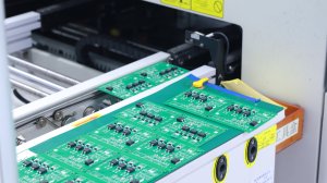
Boundary Scan JTAG Provides Non-Contact Access to Digital Nets
The core idea behind boundary scan is elegantly simple. Compliant devices include a shift-register chain at every I/O pin. When the board enters test mode, these registers disconnect the pins from the core logic and turn each pin into a controllable or observable point. A four-wire Test Access Port—TDI, TDO, TMS, and TCK—daisy-chains every compatible device on the board. A single JTAG controller can then read and write logic values across the entire interconnect without touching a single test pad.
This architecture solves the physical-access problem that cripples traditional bed-of-nails in-circuit test. On a high-density consumer PCB with micro-BGAs and 0201 passives, there may be fewer than twenty usable test pads. Boundary scan does not need them. It also scales across multi-board stacks and backplanes because the same four signals route through connectors. For digital boards dominated by FPGAs, processors, and memory, JTAG delivers structural coverage of opens, shorts, and stuck-at faults with minimal fixture investment.
Implementation begins at the schematic stage. Designers must select components that carry the IEEE 1149.1 boundary-scan cell. Most modern microcontrollers, CPLDs, FPGAs, and DDR memory controllers include the feature, but analog ICs, discrete transistors, and many power regulators do not. The test engineer then builds a netlist model called a BSDL file for each device and stitches them into a chain description. Test-pattern generation tools automatically create vectors that toggle every net and compare captured responses against expected values. The entire flow is software-driven, which makes it attractive for low-volume or rapidly evolving products.
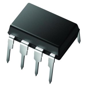
Functional Test Validates Real-World Behavior Beyond Structural Faults
Where boundary scan excels at structural verification, functional test validates behavior. A board may pass every JTAG interconnect test yet fail when powered because a decoupling capacitor is the wrong value, a reference voltage drifts with temperature, or a high-speed signal violates eye-mask margins. Functional test applies realistic stimuli—analog signals, communication protocols, load conditions—and measures whether the assembly performs to specification.
Consider a motor-drive PCB assembly. Boundary scan can confirm that the gate-driver IC is soldered correctly and that its digital control lines are not shorted. It cannot verify that the MOSFET switching edges are crisp enough, that the current-sense amplifier output is accurate within one percent, or that over-temperature shutdown triggers at the correct threshold. These parameters demand active circuitry, dynamic loads, and parametric measurement. Functional test equipment such as programmable power supplies, electronic loads, oscilloscopes, and protocol analyzers provide the necessary instrumentation.
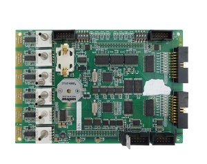
Another distinction is speed. Boundary scan shifts data serially through the chain. A full interconnect test on a board with ten devices and five thousand nets may take several minutes. Functional test, once initialized, can exercise a USB 3.0 port at full 5 Gbps or stream audio through a codec in real time. For production lines with cycle-time targets under sixty seconds, JTAG alone may be too slow for 100-percent coverage unless the chain is short or the test is partitioned across multiple stations.
Coverage Gaps Limit Boundary Scan on Mixed-Signal and Power Boards
Boundary scan is fundamentally a digital technique. It controls and observes logic levels, not analog voltages. Any net that terminates at a non-compliant device becomes invisible. On a typical IoT sensor board, the JTAG chain may reach the microcontroller and BLE module, but it cannot see the temperature sensor, the MEMS accelerometer, the battery-management IC, or the antenna-matching network. Test coverage drops sharply in these mixed-signal zones.
Power circuits present similar blind spots. Voltage regulators, DC-DC converters, and load switches rarely include boundary-scan cells. A shorted feedback resistor or an incorrect inductor value will not be detected by JTAG vectors. The same limitation applies to passive components. Resistors, capacitors, and inductors between compliant devices can sometimes be inferred by measuring pin-to-pin impedance, but this is indirect and unreliable for tightly toleranced networks.
Even within the digital domain, timing-related defects escape boundary scan. Setup-and-hold violations, crosstalk-induced jitter, and metastable states are dynamic phenomena. Boundary scan operates at the relatively slow TCK frequency and captures static logic values. It will not catch a DDR data line that fails only at the highest temperature corner or a clock line with excessive skew. These faults require at-speed functional test or specialized signal-integrity measurement.

Cost and Fixture Trade-Offs Favor Different Strategies by Volume
Test economics play a decisive role in choosing between JTAG and functional test. Boundary scan requires almost no physical fixture—just a cable to the JTAG header and software licenses for pattern generation. For prototypes, low-volume runs, or products with short life cycles, this capital efficiency is compelling. Engineering teams can bring up test coverage in days rather than weeks, and design changes only demand a software update, not a new bed-of-nails build.
Functional test, by contrast, often demands custom fixtures, interface cables, and instrumentation racks. A functional test station for an automotive ECU may cost tens of thousands of dollars and require several weeks of development. However, once built, the per-unit test time can be very short, and the coverage is deep. At volumes above ten thousand units, the amortized fixture cost drops below the recurring engineering effort of maintaining JTAG patterns for every design revision.
| Factor | Boundary Scan JTAG | Functional Test |
|---|---|---|
| Fixture cost | Low (cable + software) | High (custom hardware) |
| Setup time | Days | Weeks to months |
| Digital coverage | Excellent | Moderate |
| Analog/power coverage | None | Excellent |
| Test speed per board | Slow (serial shift) | Fast (parallel execution) |
| Best volume fit | Low to medium | Medium to high |
| Design impact | Requires compliant ICs | Requires test-point access |
The table above summarizes the central trade-offs. Neither approach dominates across all scenarios. A one-stop PCBA solution provider typically evaluates the product mix, annual volume, and defect history before committing to a test strategy.
Hybrid Test Strategies Combine JTAG with Functional and AOI Coverage
In practice, the most robust manufacturing lines layer multiple test methods. A common architecture begins with automated optical inspection after solder-paste printing and reflow. AOI catches missing components, wrong polarities, and gross soldering defects before electrical test. Next, boundary scan verifies digital interconnect integrity on the powered but unprogrammed board. This step catches opens, shorts, and wrong-component values that affect digital nets. Finally, functional test exercises the fully programmed and calibrated assembly under realistic operating conditions.
This layered approach maximizes defect detection while minimizing escape rates. JTAG acts as a fast, software-defined filter for structural digital faults. Functional test then validates the analog, power, and timing domains that JTAG cannot reach. If a defect escapes both layers, it is likely a subtle parametric or environmental issue best caught in system-level burn-in or field monitoring.
Some advanced implementations extend JTAG with vendor-specific instructions. ARM CoreSight adds serial-wire debug for processor trace. FPGA vendors provide in-system programming and logic-analyzer cores accessed through the same port. These extensions blur the line between test and debug, but they still do not replace parametric functional verification. They are complementary tools in a broader toolkit.
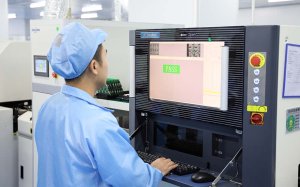
Design for Testability Decisions Lock in Coverage Early
The effectiveness of any test strategy is largely determined during design. If the BOM excludes IEEE 1149.1-compliant devices, boundary scan is impossible regardless of downstream investment. If test pads are eliminated to save board area, in-circuit test and flying-probe access disappear. If high-speed signals are routed without impedance control or length matching, functional test margins tighten.
Design-for-test guidelines therefore recommend reserving JTAG headers on every board, even if initial volumes do not justify boundary-scan deployment. The header cost is pennies; the future flexibility is substantial. Similarly, maintaining a modest set of test points for critical analog nets preserves options for flying-probe or functional test later. Documenting these decisions in the design review checklist ensures that testability is not an afterthought.
Component selection also matters. When two microcontrollers offer equivalent performance but only one includes boundary scan, the test-aware choice pays dividends during production ramp. The same logic applies to memory, interface transceivers, and power sequencers. A small premium at the component level can eliminate a large capital expense at the test station level.
Real-World Production Data Shows Where JTAG Excels and Where It Falls Short
Empirical data from high-volume electronics manufacturing illuminates the practical limits of boundary scan. In one study of telecommunications router boards, boundary scan detected approximately eighty-five percent of all manufacturing defects. The remaining fifteen percent were dominated by analog parameter drift, power-sequencing errors, and connector mechanical issues—fault classes entirely outside JTAG scope. When the same boards were subjected to combined AOI, JTAG, and functional test, the cumulative defect detection rate exceeded ninety-nine percent.
Another case involved automotive engine-control modules. Boundary scan successfully identified every open and short on the digital portion of the board, including faults beneath a 0.8 mm pitch BGA that no flying probe could reach. However, two units passed JTAG yet failed functional test because of a marginal crystal oscillator startup characteristic. The defect only manifested under cold-temperature conditions, a scenario that static boundary scan vectors cannot simulate. The experience reinforced the industry consensus: JTAG is necessary but not sufficient for mission-critical assemblies.
Consumer electronics present a different calculus. A smart-speaker board with limited analog content and a single digital signal path may achieve adequate quality with AOI plus JTAG, deferring functional test to sample-based audit. The cost savings are meaningful at volumes in the millions. The risk is that rare parametric escapes reach the field, where warranty returns are more expensive than in-factory detection. Each product category demands its own coverage-versus-cost optimization.