
BGA Assembly and X-Ray Inspection: Advanced Package Handling Guide
Ball grid array packages represent one of the most significant advances in component packaging, enabling unprecedented connection density in a compact footprint. A single BGA can provide hundreds or thousands of connections in an area that would accommodate only dozens of perimeter-leaded devices. However, this density comes with BGA assembly challenges that require specialized equipment, processes, and inspection capabilities.
This guide covers the critical aspects of BGA assembly, from placement through reflow and inspection, with practical guidance for engineers and manufacturing teams working with these advanced packages.
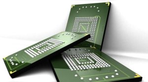
Understanding BGA Package Variations
Ball grid arrays come in several configurations, each with different assembly considerations. Plastic ball grid arrays use a plastic overmolded substrate with solder balls on the bottom. Ceramic ball grid arrays use a ceramic substrate for superior thermal performance and are common in high-reliability applications. Tape ball grid arrays use a flexible tape substrate that allows the package to conform slightly to the board surface.
The pitch, or spacing between adjacent solder balls, is a critical parameter. Standard BGA pitches range from 1.0mm to 1.27mm and are relatively straightforward to assemble. Fine-pitch BGA packages, with pitches of 0.8mm, 0.65mm, or even 0.5mm, require more precise process control at every stage. The smaller solder balls and tighter geometry leave less margin for placement error, paste printing variation, and reflow profile deviation.
Package body size also affects assembly complexity. Larger packages, exceeding 35mm on a side, are susceptible to warpage during reflow. As the package and board heat unevenly, differential expansion can cause the corners to lift or compress, distorting the solder ball array and causing opens or bridges. Package warpage is one of the most common causes of BGA assembly defects on large packages.
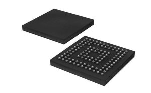
Solder Paste Printing for BGA Pads
Solder paste printing is critical for BGA assembly. The paste deposit on each BGA pad must have the correct volume to form a reliable solder joint. Too little paste results in insufficient solder, cold joints, or opens. Too much paste causes solder bridging between adjacent balls, particularly on fine-pitch packages. The acceptable paste volume range narrows as pitch decreases.
Stencil design for BGA pads typically uses aperture sizes that match or slightly reduce the pad diameter. The stencil thickness must balance the paste volume needed for BGA pads against the requirements of other component types on the same board. A common approach uses a standard 0.12mm or 0.15mm stencil for the entire board, with BGA apertures sized to deliver appropriate paste volume at that thickness.
For fine-pitch BGA packages, step-down stencils may be used. These stencils are selectively thinned in the BGA area, reducing paste deposit volume for fine-pitch pads while maintaining standard thickness for larger components. Step-down stencils add cost but are often necessary for mixed-pitch assemblies where a single stencil thickness cannot satisfy all component requirements.
Solder paste inspection is particularly important for BGA pads because the hidden nature of the joints means printing defects cannot be detected by visual inspection after reflow. SPI systems verify paste volume, height, and registration for every BGA pad before components are placed, enabling corrective action while the defect is still easy to fix.
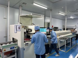
BGA Placement Accuracy Requirements
BGA placement requires high accuracy, but the tolerance is more forgiving than many engineers expect. Because solder balls reflow into a liquid state, surface tension tends to self-align the package to the pad pattern. As long as the placement is within approximately one-third of the ball pitch, the package will self-align during reflow.
However, this self-alignment has limits. Placement errors exceeding half the ball pitch can cause solder bridging between adjacent pads or insufficient contact on displaced balls. Fine-pitch packages have less self-alignment tolerance because the balls are smaller and the gaps between them are narrower. Modern placement machines achieve accuracy of 25 microns or better, which is sufficient for all but the finest pitch BGA packages.
Placement force is another consideration. BGA packages, particularly large ones, can be damaged by excessive placement force. The machine must apply enough force to embed the solder balls into the paste deposits for adequate contact, but not so much that the package substrate flexes or the balls are deformed. Placement force settings should be developed based on the specific package and validated during first-article inspection.
The vision system on the placement machine must be configured correctly for BGA packages. The system uses the solder ball pattern to verify package identity and determine placement orientation. For packages with symmetric ball patterns, an additional marking or fiducial on the package top is used to determine rotational orientation. Incorrect vision system configuration can cause the package to be placed rotated or mirrored, a defect that is expensive to detect and correct after reflow.

Reflow Profile Development for BGA Assemblies
The reflow profile for BGA assembly must account for several factors unique to these packages. The thermal mass of the package body creates a temperature lag between the board surface and the solder balls underneath. Thermocouples attached to the board surface may read a significantly different temperature than the actual solder ball temperature, leading to incorrect profile settings.
For accurate profiling, thermocouples should be attached at locations that represent the BGA thermal environment. This includes a thermocouple on a pad adjacent to the BGA, another on the BGA package surface, and for critical applications, a thermocouple attached to a sacrificial solder ball underneath the package. The profile is developed to ensure the solder balls reach the required peak temperature for adequate time without exceeding the package’s maximum temperature rating.
Nitrogen atmosphere reflow is strongly recommended for BGA assembly. The reduced oxygen environment improves solder wetting on the BGA pads and balls, reduces oxidation of the solder surfaces, and significantly reduces voiding in the finished joints. The cost of nitrogen is easily justified by the improvement in BGA joint quality and the reduction in rework.
Voiding: Causes and Mitigation
Voiding, the presence of gas pockets within solder joints, is a common concern in BGA assembly. Voids form when flux volatiles become trapped in the molten solder and cannot escape before the solder solidifies. Small voids, typically below 25 percent of the joint area, are generally acceptable per IPC-7095. Larger voids can compromise joint mechanical strength, thermal conductivity, and electrical performance.
Several factors influence voiding levels. Solder paste formulation is significant; pastes designed for BGA applications produce fewer voids. Reflow profile affects voiding; longer soak times allow more flux volatiles to escape before the solder melts. Pad design matters; pads with thermal vias can wick solder away from the joint and create voids if the vias are not filled. And component preparation plays a role; BGA packages that have absorbed moisture may release steam during reflow, creating voids.
Mitigation strategies include using low-voiding solder paste formulations, optimizing the reflow profile with extended soak times, designing pads with plugged thermal vias, baking moisture-sensitive BGA packages before assembly, and using vacuum reflow systems that actively remove gas from the joint during the liquidus phase. Vacuum reflow can reduce voiding to single-digit percentages but requires specialized equipment and adds cycle time.
X-Ray Inspection: The Essential Tool for BQA
Because BGA solder joints are hidden beneath the package body, visual inspection is impossible. X-ray inspection is the only reliable method for evaluating BGA joint quality in production. X-ray systems penetrate the package and board materials to reveal the solder joints, allowing inspectors to assess solder coverage, voiding, ball shape, and bridging.
Two-dimensional X-ray systems provide a top-down view of the joint array. They are effective for detecting bridging, missing balls, and large voids. Three-dimensional X-ray systems, also called computed tomography or laminography systems, can slice through the joint at different heights, providing detailed information about void distribution, joint shape, and pad wetting. For high-reliability applications, 3D X-ray inspection is becoming standard practice.
X-ray inspection programs should be developed for each BGA type on the assembly. The program defines the inspection parameters, acceptance criteria, and defect detection algorithms. Automated X-ray inspection systems can process boards at production-line speeds, flagging defects for operator review. For lower volumes, manual X-ray inspection by trained operators is adequate but requires significantly more time per board.

When evaluating a PCB assembly manufacturer for BGA work, verify their X-ray inspection capability, ask to see voiding data from recent BGA assemblies, and request sample X-ray images. A manufacturer with robust BGA processes will have well-documented inspection criteria and voiding trend data. A qualified PCBA partner with advanced BGA capabilities provides the equipment, processes, and engineering expertise needed to achieve reliable BGA assembly at production volumes.