

The most expensive phase of PCB assembly is not manufacturing but rework caused by designs that were not optimized for production. PCB assembly design guidelines, properly applied during layout, eliminate the vast majority of assembly defects before a single board is built. The payoff is higher first-pass yield, lower production cost, and faster time-to-market.
This handbook consolidates the most impactful DFM rules across component placement, pad design, thermal management, and panelization. Each guideline is based on IPC standards and validated production experience, not theoretical best-case scenarios.

Component Placement Rules That Prevent Defects
Edge Clearance and Panel Considerations
Components should maintain a minimum clearance of 3mm from the board edge for panelized assemblies. This buffer zone protects components from mechanical stress during depaneling, whether by routing, scoring, or punching. For ceramic capacitors, which are particularly susceptible to micro-cracking from mechanical stress, increase the edge clearance to 5mm where possible.
The depaneling method should influence placement decisions at the design stage. V-scored panels concentrate stress along the score line, making it inadvisable to place sensitive components near these areas. Routed panels with tab connections apply less stress but require clearance for the router bit diameter. Discuss the intended depaneling method with your assembly partner before finalizing component placement.

Orientation and Polarity Consistency
All polarized components, including diodes, electrolytic capacitors, and ICs, should share a consistent orientation across the board. When all polarized components face the same direction, visual inspection for correct orientation is faster and more reliable. The operator or AOI system verifies one pattern rather than checking every component individually.
Similarly, all chip components of the same size should ideally be oriented in the same direction. This consistency simplifies the pick-and-place program, reduces head rotation during placement, and slightly improves placement speed. For wave-soldered assemblies, component orientation relative to the wave direction becomes an additional consideration to prevent shadowing.
Thermal Balance and Reflow Considerations
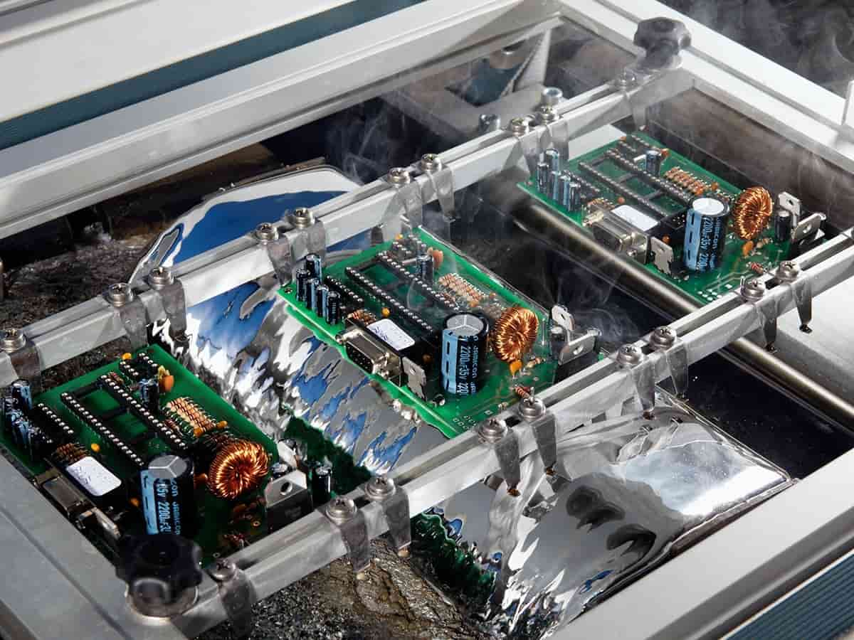
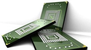
Components with significantly different thermal mass should not be clustered together. A large BGA next to a small chip capacitor creates uneven heating during reflow. The BGA acts as a heat sink while the small component heats rapidly, potentially leading to cold joints on one and component damage on the other.
Distribute large, thermally massive components across the board area rather than concentrating them in one zone. If high-mass components must be adjacent to lightweight components, work with your assembly partner to develop a reflow profile that accommodates both. Thermocouple profiling during prototype runs will confirm whether the profile achieves adequate soldering on all components.
Pad Design: The Foundation of Reliable Solder Joints
Pad geometry directly determines solder joint quality, and poor pad design is impossible to correct during assembly. The following guidelines prevent the most common pad-related defects.
Follow IPC-7351 land pattern dimensions rather than component manufacturer recommendations when they differ. IPC standards are validated for high-yield assembly processes, while component datasheet footprints are sometimes optimized for hand soldering or prototyping. Use the density level appropriate for your application: Level A for maximum reliability, Level B for general purpose, or Level C for high-density designs.
Set solder mask clearance correctly. The solder mask opening should be 0.1mm larger than the copper pad on each side. Tighter clearances risk solder mask encroachment onto the pad, reducing the solderable area. Larger clearances risk exposing adjacent traces and creating solder bridging. For fine-pitch devices below 0.5mm pitch, solder mask defined pads may be preferable, where the mask opening defines the solderable area rather than the copper geometry.
Include thermal relief on pads connected to copper planes. Direct connections from component pads to large copper areas act as heat sinks during reflow, preventing the pad from reaching soldering temperature. Thermal relief pads use spokes to connect the pad to the plane while limiting thermal conductivity. The standard thermal relief uses four spokes, each 0.25 to 0.3mm wide for typical SMT pads.

Via Design and Placement
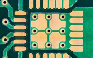
Vias placed within SMT pads create several problems. Solder wicks down the via hole during reflow, starving the joint of solder. The via also traps flux residue that can cause long-term corrosion. For these reasons, via-in-pad should be avoided unless absolutely necessary, and when used, the vias must be filled and capped before assembly.
For vias adjacent to pads, maintain a minimum 0.25mm distance from the pad edge. Closer vias risk solder bridging between the pad and the via during reflow, particularly if the via is untented. Tenting vias with solder mask eliminates this risk and is recommended for vias within 0.5mm of component pads.
Fiducial Marks: Simple but Essential
Fiducial marks are reference points that allow the pick-and-place machine and AOI system to establish the board’s exact position and orientation. Global fiducials, typically three marks near the board corners, provide overall board registration. Local fiducials near fine-pitch components provide additional precision for critical placements.
Fiducial design requirements are straightforward: 1mm diameter circular copper pad, surrounded by a clear area at least twice the fiducial diameter, with no solder mask coverage. Place fiducials on both sides of double-sided assemblies. For panelized designs, include fiducials on both the panel rails and individual board images.

Panelization Strategy
Panelization, the arrangement of multiple boards into a single assembly panel, is often an afterthought in the design process but has significant implications for assembly efficiency and quality. A well-designed panel maximizes board utilization, provides adequate support for assembly processes, and enables clean depaneling.
For SMT assembly, the panel must include rails for conveyor transport, typically 5 to 10mm wide along two parallel edges. The rails provide space for tooling holes, fiducial marks, and panel identification. Components should not be placed within 3mm of the panel edge, as this area is consumed by conveyor rails and may be subject to mechanical stress.
Board-to-board spacing within the panel depends on the depaneling method. Routed panels require approximately 2mm between boards for the router bit. V-scored panels need less spacing but the score depth must be precisely controlled to avoid cutting too deeply or too shallowly. Discuss panelization with your PCB assembly manufacturer before finalizing the design, as their equipment and processes may impose additional requirements.
Applying these DFM guidelines during layout, rather than discovering violations during manufacturing review, is the most cost-effective investment a design team can make. A professional PCBA partner will provide design review feedback that helps engineers internalize these rules for future projects, building institutional knowledge that improves every subsequent design.
