
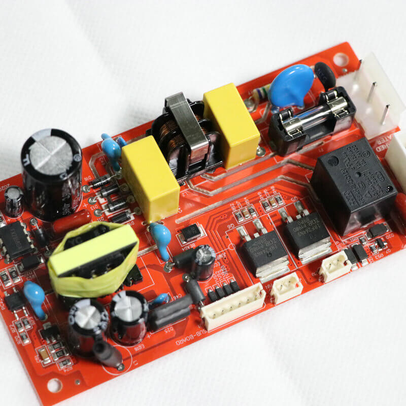
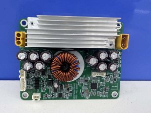
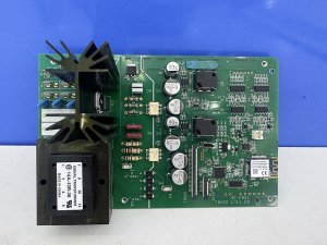
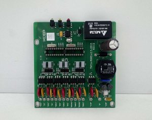
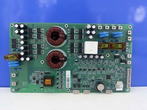
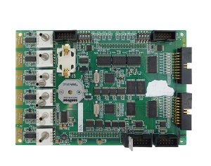
As the core carrier of modern communication equipment, PCBA (Printed Circuit Board Assembly) continuously propels innovation in devices for 5G, IoT, intelligent transportation, and other fields through technological advancements such as high-density integration, high-speed signal transmission, and smart manufacturing. This article systematically analyzes PCBA’s technological driving force, production optimization pathways, application scenario expansion, and reliability assurance systems within the communications industry, providing in-depth reference for electronic manufacturing and communication engineering sectors.
1.Technological Innovation Drivers: Core Breakthroughs in PCBA
1.1 High-Density Integration Technology
Technical Feature Analysis:
High-density integration achieves miniaturization breakthroughs through three pathways. Microfabrication processes employ precision line-making techniques, achieving micron-level accuracy in line width and spacing. Multi-layer stacking technology overcomes traditional layer count limitations, enabling high-density interconnections from 12 to over 40 layers. Advanced packaging integrates System-in-Package (SiP) and 3D-IC technologies, vertically stacking multifunctional units like processors, memory, and RF modules within a single component.
5G Communication Equipment Application Examples:
In 5G base stations and terminal devices, high-density integration technology resolves spatial constraints in the millimeter-wave frequency band. By tightly packing baseband processing units, RF front-end modules, and power management modules, device volume is reduced by over 40% while supporting gigabit-per-second data transmission rates, ensuring efficient and stable operation of large-scale MIMO antenna systems.
1.2 High-Speed Transmission and Signal Integrity
Key Technology Breakthroughs:
High-speed transmission line design employs differential pair routing, impedance control, and back-drilling techniques to support high-speed interface standards like PCIe 5.0, USB4, and 100G Ethernet. High-frequency signal processing technology addresses 5G millimeter-wave and Sub-6GHz band requirements. By utilizing low-loss substrates (e.g., Megtron 6, Rogers RO4350B) and optimized laminate design, signal attenuation is controlled within 0.5dB per inch.
Performance Enhancement Value:
High-speed transmission technology not only elevates core performance metrics of communication equipment but also establishes the hardware foundation for emerging application scenarios. It enables low-latency access for massive IoT devices, facilitates real-time data exchange for vehicle-road coordination in intelligent transportation, and ensures high-speed data throughput for model inference in AI edge computing scenarios.
2.Manufacturing Optimization: Intelligent and Green Transformation
2.1 Automated Smart Manufacturing
Intelligent Equipment System:
PCBA production lines fully integrate high-speed pick-and-place machines (achieving speeds exceeding 150,000 components per hour), automatic optical inspection (AOI) equipment, X-ray inspection systems, and intelligent warehousing logistics systems. Industrial robots handle material loading/unloading, component insertion, and testing processes, enabling 24/7 continuous production. A big data analytics platform collects real-time equipment operating parameters, using machine learning algorithms to predict maintenance needs and quality fluctuation trends.
Performance Enhancement Dimensions:
Intelligent management reduces production changeover time by 60%, increases first-pass yield to over 98%, and lowers energy consumption per unit of output by 25%. A digital quality traceability system enables full lifecycle data visibility for individual products, providing process assurance for the high reliability requirements of communication equipment.
2.2 Environmental and Green Manufacturing Practices
Clean Production Processes:
Comprehensive adoption of lead-free soldering technology (SAC305 and other lead-free solders) complies with RoHS 2.0 and REACH regulations. Introduction of low-oxidation processes like nitrogen-shielded reflow soldering and selective wave soldering reduces flux usage by over 30%. Cleaning processes transition to water-based and semi-water-based solutions, replacing traditional solvent cleaning.
Sustainable Value:
Green manufacturing measures significantly reduce carbon emissions and hazardous substance discharges during production, advancing the telecommunications industry’s carbon neutrality goals. Environmentally compliant PCBA products gain international market access, helping communication equipment manufacturers overcome green trade barriers and achieve sustainable global supply chain operations.
3. Application Expansion: From Consumer Electronics to Infrastructure
3.1 Smartphones and Communication Base Stations
Smartphone Innovation Enablement:
PCBA technology drives high-level integration of functional modules in smartphones. Motherboards integrate complex features like 5G baseband chips, Wi-Fi 6E modules, multi-camera image signal processors, and fast-charging management units to deliver flagship-level performance within limited space. High-Density Interconnect (HDI) technology employs Any Layer interconnection solutions to support structural demands of innovative form factors like foldable phones.
Core Component Role in Base Stations:
Within mobile communication base stations, PCBA serves as the core carrier for baseband processing units (BBU), radio remote units (RRU), and antenna filter modules. High-frequency, high-speed boards and multilayer lamination processes ensure stable transmission of 28GHz millimeter-wave signals, while thermal management designs and high-reliability soldering guarantee long-term operation in harsh outdoor environments.
3.2 IoT and Intelligent Transportation
Core of IoT Devices:
As the central control unit for IoT terminal devices, PCBA integrates microcontrollers, wireless communication modules (NB-IoT, LoRa, Zigbee), sensor interfaces, and power management functions. Low-power design technology extends device battery life to 5–10 years, enabling large-scale deployment across massive application scenarios like smart cities, industrial monitoring, and agricultural sensing.
Empowering Intelligent Transportation Systems:
In the Vehicle-to-Everything (V2X) domain, PCBA technology underpins the high-reliability operation of On-Board Units (OBUs) and Roadside Units (RSUs). Autonomous driving control units employ high-layer-count and rigid-flex PCB designs to withstand vehicle vibration, thermal cycling, and other demanding environmental conditions. Intelligent traffic signal control systems leverage PCBA to enable real-time traffic flow sensing and optimized scheduling, boosting road capacity efficiency by over 20%.
4.Safety and Reliability Assurance System
4.1 Safety Performance Design
Multi-layered Protection Mechanisms:
PCBA design incorporates overvoltage protection, overcurrent protection, and electrostatic discharge (ESD) circuits to prevent damage from abnormal electrical stresses. Triple-proof coating processes (acrylic, polyurethane, or silicone materials) provide moisture, mold, and salt spray resistance, suitable for coastal and high-humidity deployments. Safety certification complies with IT equipment safety standards including IEC 62368 and UL 60950.
Electromagnetic Compatibility Optimization:
Power integrity (PI) and signal integrity (SI) are designed synergistically to control electromagnetic radiation and susceptibility. Shielding enclosures, filtering circuits, and optimized grounding ensure compliance with EMC standards like CISPR 32 and EN 301 489, guaranteeing stable operation in complex electromagnetic environments.
4.2 Reliability Verification System
Comprehensive Testing Process:
PCBA products undergo Functional Component Test (FCT) to validate logic functionality, In-Circuit Test (ICT) to inspect component parameters and soldering quality, and Burn-in testing to screen out early-failure products. Environmental reliability testing includes rigorous validation such as temperature cycling (-40°C to 125°C), mechanical vibration, shock testing, and Highly Accelerated Life Testing (HALT).
High-Standard Alignment for Telecommunications:
To meet the 99.999% availability requirement for communication equipment, PCBA Mean Time Between Failures (MTBF) is designed to exceed 100,000 hours. Strict process capability control (CPK ≥ 1.67) is implemented, with 100% automated inspection at critical processes, ensuring products meet network certification and long-term operational requirements of telecom carriers.
5.Future Outlook
As the core component in modern communication equipment manufacturing, PCBA is accelerating industry transformation through continuous technological innovation, smart manufacturing upgrades, deep application scenario development, and enhanced reliability systems. For frontier applications like 6G pre-research, satellite internet, and computing power networks, PCBA will evolve toward higher density, higher frequency, and greater reliability, providing a robust hardware foundation for the thriving digital economy.