

Thermal Management Protects Components From Overheating in PCB Assembly
Every active device on a printed circuit board converts part of its consumed electrical power into heat, and without deliberate thermal management for PCB assembly that heat accumulates until junction temperatures climb past the ratings set by component manufacturers. A modern high-density board can pack dozens of power regulators, processors, and driver ICs into a few square centimetres, so the margin between a stable product and a failing one is often decided by how effectively the assembly sheds heat. When temperatures stay within specification, solder joints remain mechanically sound, dielectric materials resist breakdown, and semiconductor life expectancy follows its rated curve. When they do not, premature wear-out, intermittent faults, and field returns follow.
A competent PCB assembly manufacturer treats thermal design as an early engineering task rather than a late fix, because reworking a board that already suffers from hotspots is far more expensive than placing copper and vias correctly the first time. This article explains the practical techniques that keep an assembled board cool enough to last.
Copper Pours and Thermal Planes Spread Heat Across the Board
One of the most cost-effective thermal management steps in PCB assembly is simply giving heat somewhere to go. A wide copper pour connected to a hot component lead acts like a small heat sink built into the board itself, spreading energy across a larger area so the local temperature rise stays modest. Internal copper planes, especially ground and power planes on multilayer stacks, form low-resistance thermal paths that distribute heat toward the board edges and any attached enclosure.
Designers typically size these pours using the same rules that govern current-carrying capacity, because the copper that conducts amps also conducts watts. A thicker copper weight, such as two-ounce or three-ounce foil instead of the default one ounce, roughly doubles or triples the cross-sectional area available for both electrical and thermal flow, making it a favourite trick for power-dense assemblies where every degree of junction temperature matters.
Thermal Vias Carry Heat Away From Surface-Mounted Power Devices
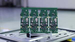
Many power devices are surface-mounted with a thermal pad on the bottom that cannot radiate directly into the air, so the only escape route is downward through the board. Thermal vias, small plated holes arranged in an array under that pad, bridge the surface layer to inner copper planes or to a bottom-side heatsink, dramatically lowering the thermal resistance between the die and the ambient environment. A well-designed thermal via array can cut junction-to-board resistance by more than half compared with a pad that has no vias at all.
Best practice in PCB assembly calls for filling or at least tenting these vias to prevent solder from wicking down the hole during reflow, which would starve the joint and create voids. The trade-off between unfilled vias that conduct heat well and filled vias that solder cleanly is one of the routine judgements a competent assembly house makes on every power layout.

Heatsinks and Thermal Interface Materials Cool High-Power Components
When a component dissipates more power than the board alone can handle, an external heatsink becomes necessary, and the thermal interface material, or TIM, that joins it to the package is often the weakest link in the chain. Air is a poor conductor, so a bare metal-to-metal contact leaves microscopic gaps that trap heat; a thin layer of thermally conductive grease, pad, or phase-change material closes those gaps and can improve heat transfer by a wide margin. Selecting the right TIM means balancing conductivity, ease of assembly, and long-term pump-out resistance under thermal cycling.
Clip-on, screw-down, and bonded heatsinks each suit different production volumes and enclosure constraints. In high-volume PCB assembly, a push-pin or spring-clip attachment is faster on the line, while low-volume or high-reliability builds may use a bonded interface for a permanent, gap-free bond that survives years of temperature swing.
Component Placement and Layout Reduce Thermal Hotspots in Assembly
Where parts sit on the board matters as much as how they are cooled. Clustering several heat-generating devices in one corner creates a thermal hotspot that no amount of copper can fully rescue, whereas spreading them across the surface lets the whole board act as a heat spreader. Sensitive analog and timing components should be placed away from power stages, and exhaust paths should be kept clear of components that cannot tolerate warmth.
A few layout habits consistently improve thermal outcomes:
- Separate high-power regulators from precision reference and sensor circuitry.
- Orient tall heatsinked parts to align with natural or forced airflow direction.
- Keep thermal relief on through-hole pads to avoid solder starvation during assembly.
- Place temperature sensors near the components most likely to overheat.
- Avoid routing signal traces across large copper pours that alter controlled impedance.
Trace Width and Copper Weight Set Safe Current Limits
The copper traces that carry current also generate heat through I-squared-R losses, and an undersized trace rapidly becomes the hottest point on an assembled board. Estimating the right trace width depends on the allowed temperature rise, the copper weight, and the continuous current, with industry reference charts providing a starting point that experienced layout engineers then adjust for stacking and ambient conditions. For power rails that exceed a few amperes, designers often replace narrow traces with poured copper and reinforce them with extra via stitching.
The table below summarises how copper weight and trace width combine to raise the safe current a typical outer-layer trace can carry before its temperature climbs by twenty degrees Celsius:
| Copper weight (oz) | Trace width (mm) | Approx. current at +20 C rise (A) |
|---|---|---|
| 1 | 0.5 | 1.4 |
| 1 | 1.0 | 2.4 |
| 2 | 1.0 | 3.8 |
| 2 | 2.0 | 6.0 |
| 3 | 2.0 | 8.5 |
These figures are planning estimates only; a final design should always be verified against the actual stack-up, ambient temperature, and cooling method used in production.
Reflow Thermal Profiling Safeguards Temperature-Sensitive Parts
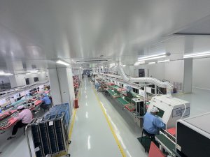
Thermal management does not stop at the design stage; it continues on the assembly line, where the reflow oven profile decides whether a board survives soldering intact. A correct profile ramps the assembly gradually, soaks it to activate flux, peaks briefly within the solder’s liquidus window, and cools in a controlled slope that prevents thermal shock. Components rated for lower peak temperatures, such as some connectors and LEDs, must be placed in oven zones where the local heat stays within their limit, or the board needs a dual-profile or local shielding approach.
A one-stop PCBA solution provider typically measures the actual profile with thermocouples attached to representative boards before a production run, because the theoretical oven setting and the real component temperature can differ by tens of degrees depending on board mass and density. That measured data is what protects both the solder joints and the heat-sensitive parts.
Enclosure and Airflow Design Completes the Thermal Path
No board is an island, and the enclosure around it decides whether the heat removed by copper and vias actually leaves the product. Natural convection relies on warm air rising and drawing cooler air in through vents, which works for low-power assemblies but stalls in sealed or densely packed housings. Forced convection with a fan moves a controlled volume of air across the board and can lower component temperatures by a substantial margin even at modest flow rates. Vent placement, fan sizing, and the avoidance of internal obstructions are therefore part of thermal management for PCB assembly, not an afterthought handled by mechanical engineering alone.
In sealed or outdoor units, conduction to the enclosure wall through standoffs and thermal pads often replaces airflow entirely, turning the metal housing into the final heatsink. Coordinating the PCB layout with the mechanical envelope early prevents the common late-stage surprise of a board that is perfectly cooled in open air yet overheats the moment it is installed.
Thermal Design Validation Confirms PCB Assembly Reliability
Good intent is not the same as a cool board, so thermal validation closes the loop. Infrared thermography during a powered test reveals hotspots that schematic review would never predict, while thermal chamber cycling confirms the assembly survives the temperatures it will meet in the field. For high-reliability markets, these tests are paired with stress screening so that weak joints and marginal layouts fail in the factory rather than in the customer’s hands.
Documentation of the thermal budget, expected power, estimated junction temperature, and measured results, also gives downstream teams confidence and shortens any future failure analysis. Treating thermal management as a measured specification rather than a hopeful guess is what separates a board that merely works from one that lasts for years.
Summary
Thermal management for PCB assembly is the discipline of moving heat away from sensitive components through copper pours, thermal vias, heatsinks, careful layout, and correctly sized traces, then confirming the result with profiling and testing. When these techniques are applied early and verified on the line, solder joints stay intact, components run within rating, and the finished product delivers the reliability its design promised.
FAQ
What is the most cost-effective thermal management technique in PCB assembly?
Widening copper pours and adding thermal vias under power devices costs almost nothing in materials yet removes a large share of localized heat, which makes it the first technique most assembly engineers apply before considering external heatsinks.
How do thermal vias avoid solder defects during reflow?
Bare thermal vias can pull solder away from the pad and form voids, so they are normally tented, filled, or plugged. Filled vias give the cleanest joint and the best heat path, while tented vias are cheaper and still prevent wicking on most layouts.
Why does copper weight matter for both current and heat?
Copper that carries electrical current also conducts thermal energy, so a heavier foil such as two-ounce or three-ounce copper both raises the safe ampacity of a trace and improves its ability to spread heat away from hot spots.
Can reflow soldering damage temperature-sensitive components?
Yes, if the oven profile exceeds a part’s rated peak temperature the component can crack or drift out of specification, which is why a measured thermal profile and careful zone placement are standard practice before any production run.
How is thermal performance verified after assembly?
Infrared thermography under load and thermal chamber cycling are the common validation methods, often combined with stress screening so marginal joints reveal themselves in the factory rather than during field use.