
PCB Assembly for IoT Devices: Manufacturing the Connected World
The Internet of Things has created a new category of electronic products with manufacturing requirements that differ from traditional electronics. IoT devices combine sensors, wireless communication, processing, and power management in compact, cost-sensitive packages produced at varying volumes from thousands to millions of units. PCB assembly for IoT devices demands specific design and manufacturing approaches that address these unique requirements.
This guide examines the manufacturing challenges specific to IoT electronics, from RF-sensitive assembly processes to volume scalability, and provides practical guidance for product teams bringing IoT devices to market.

Miniaturization and High-Density Assembly
IoT devices are typically small, often small enough to fit within a smartphone footprint or smaller. This size constraint drives board design toward high-density interconnect technology, fine-pitch components, and multi-layer stackups that maximize routing capacity in minimal area. The assembly process must handle 0201 or even 01005 passive components, fine-pitch ICs with 0.4mm or finer pitch, and package-on-package configurations that stack multiple devices vertically.
High-density assembly requires equipment and processes calibrated for precision. Solder paste printing must achieve consistent deposit volumes on pad geometries measured in tens of microns. Pick-and-place machines must position components with accuracy measured in microns rather than tens of microns. Reflow profiles must be developed with thermocouples placed at multiple locations to ensure uniform heating across the small but dense board area.
The cost of high-density assembly equipment and the expertise to operate it effectively means that IoT product teams should work with assembly partners who have proven fine-pitch and HDI experience. A manufacturer whose standard capability stops at 0402 components and 0.5mm pitch will struggle with the density requirements of modern IoT designs.
Package-on-Package Assembly
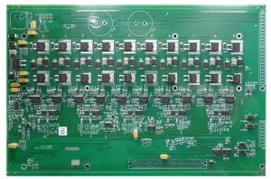
Package-on-package technology stacks two or more components vertically, connecting them through solder balls between the stacked packages. This approach is common in IoT devices where a processor and memory are stacked to save board area. PoP assembly requires specialized equipment that can place the bottom package, flux the solder balls, place the top package, and reflow both simultaneously.
The process control requirements for PoP are stringent. Excessive flux can cause bridging between the stacked solder balls. Insufficient flux causes poor wetting and open connections. Placement accuracy must be high enough to align the top package with the bottom package’s ball pattern. And the reflow profile must accommodate the thermal mass of both packages, which is higher than either package individually.
Wireless Integration and RF Considerations
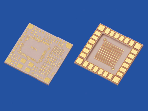
Most IoT devices include wireless communication capabilities, whether Wi-Fi, Bluetooth, Zigbee, LoRa, or cellular connectivity. These wireless functions impose specific requirements on the PCB design and assembly process that go beyond standard digital electronics.
RF circuitry requires controlled impedance traces for antenna feeds and transmission lines. The impedance is determined by the trace geometry, dielectric thickness, and material properties. During assembly, any process that affects these parameters can degrade RF performance. Solder mask thickness on RF traces, copper roughness on trace edges, and component placement near antenna structures all influence impedance and signal integrity.
Antenna integration is another IoT-specific challenge. PCB trace antennas, chip antennas, and external antennas all require different assembly considerations. Trace antennas must be manufactured to tight dimensional tolerances because the trace geometry determines the antenna’s resonant frequency. Chip antennas must be placed accurately because their position relative to ground planes affects performance. The assembly process must not add solder mask or coating material over antenna structures, as this can detune the antenna.
RF testing during production is essential for IoT devices. Network analyzer measurements verify antenna matching and resonance. Conducted power measurements verify transmitter output. Sensitivity measurements verify receiver performance. These tests require specialized equipment and test fixtures, adding to the test development effort and production cycle time.
Power Management and Battery Integration
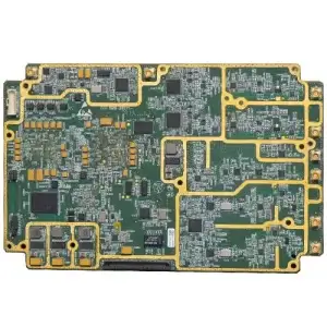
IoT devices are often battery-powered, making power efficiency a primary design driver. The PCB assembly process can affect power consumption in several ways. Leakage currents from flux residue on high-impedance nodes can drain batteries prematurely. Poor solder joints on power management ICs can introduce resistance that wastes power. And component placement affects thermal management, which influences the efficiency of switching regulators.
Cleanliness standards for battery-powered IoT devices should be higher than for mains-powered products. No-clean flux residues that are acceptable for many applications may create leakage paths that drain batteries in ultra-low-power designs. Cleaning processes, whether aqueous or solvent-based, should be validated through ionic contamination testing to verify that residues are below acceptable thresholds.
Battery integration presents its own assembly challenges. Battery connectors must provide reliable contact while allowing for battery replacement or servicing. Battery management circuits must be assembled with components rated for the battery’s voltage and current characteristics. And in devices with embedded batteries, the assembly process must accommodate battery installation without exposing the battery to reflow temperatures or cleaning chemicals.

Volume Scalability: From Prototype to Mass Production
IoT products often follow a rapid scaling trajectory from prototype through pilot production to high-volume manufacturing. The PCB assembly process must scale accordingly, which is easier when the same manufacturing partner can support all volume stages.
During prototyping, flexibility and speed are paramount. The assembly partner should be able to process small batch builds quickly, accommodate design iterations without significant setup costs, and provide engineering feedback to improve manufacturability. Quick-turn assembly services that deliver boards in days rather than weeks are valuable during this phase.
During pilot production, the focus shifts to process optimization and yield improvement. The assembly partner should work with your team to refine the process, optimize stencil design, develop test strategies, and build the documentation needed for volume production. Statistical process control data from pilot runs establishes the baseline for volume production quality targets.
During volume production, efficiency and consistency become the priorities. The assembly partner must maintain quality while processing large volumes, manage component sourcing for uninterrupted supply, and provide the data and reporting needed to monitor production health. The ability to support all three stages ensures continuity and avoids the quality dips that often accompany partner transitions.
Certification and Compliance
IoT devices require multiple certifications before market entry. FCC, CE, and other regional radio certifications verify that wireless emissions comply with regulatory limits. These certifications require specific test samples, and the assembly process must produce samples that are representative of production units. Process variations between prototype and production can cause certification failures if the production process differs significantly from the prototype process.
Material compliance is another consideration. RoHS and REACH compliance requires verification that all materials, including solder, laminate, and component finishes, meet regulatory requirements. The assembly partner should maintain material compliance documentation and provide declarations of conformity for all materials used in the assembly.
For consumer IoT products, safety certifications such as UL or IEC may be required, particularly for devices that include battery charging circuits. The assembly process must be documented and controlled to support these certifications, with traceability that links finished products to specific material lots and process records.

Bringing an IoT device to market requires a PCB assembly manufacturer who understands the unique challenges of connected devices, from RF-sensitive assembly to volume scalability. A partner with IoT manufacturing experience provides the equipment, processes, and engineering support needed to produce reliable, certifiable products at competitive cost and at the volumes your market demands.