
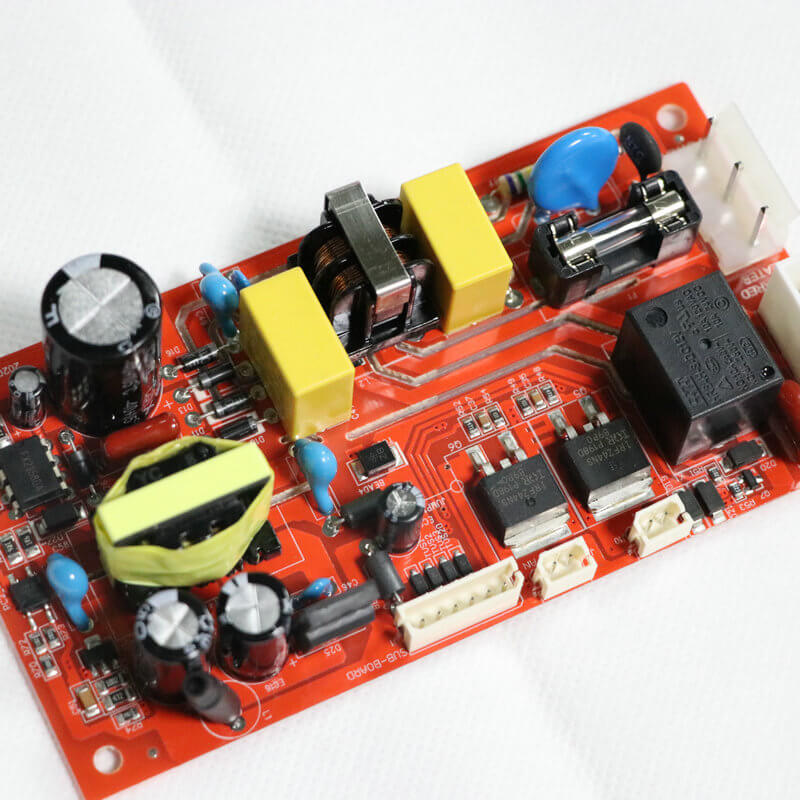
PCBA manufacturing encompasses the entire process from PCB design and manufacturing, component procurement, SMT placement, DIP insertion, soldering and assembly, functional testing, through to packaging and delivery. This article analyses the key points of each stage, typical scheduling and quotation strategies, to assist clients in planning production, controlling costs and ensuring quality.
1.PCB Design and Manufacturing
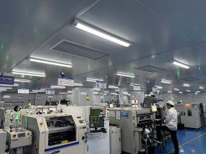
The PCB forms the foundation of the entire PCBA, with its design determining the product’s functionality and performance. Its role is to provide connections and support for components, ensuring the circuit operates correctly. The process includes schematic design, layout and routing, board material selection, and manufacturing. Once the design is complete, the PCB undergoes multiple manufacturing stages, including etching, drilling, and pad treatment.
2.Component Procurement
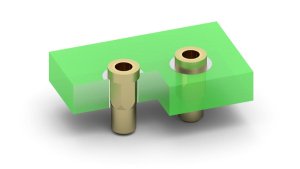
The selection of electronic components directly impacts product performance and cost. The role is to source the necessary electronic components for the PCBA. The process involves procuring components that meet the requirements based on the client’s Bill of Materials (BOM), whilst ensuring the supplier’s qualifications and the consistent quality of the components.
3. SMT Placement and DIP Insertion
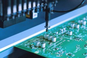
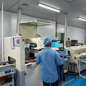
This is the core stage of PCBA manufacturing. SMT placement involves mounting electronic components onto the surface of the PCB, which is suitable for small components. DIP insertion is suitable for larger components or those with specific functions, and is completed via wave soldering or manual soldering.
4.Soldering and Assembly Stage
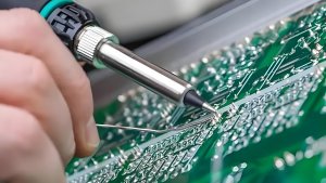
This stage completes the mechanical and electrical connections of the components. Its purpose is to ensure that each component is securely and reliably connected to the PCB. The process includes reflow soldering, wave soldering and manual soldering, with the appropriate method selected according to the type of component.
5.Functional Testing and Quality Inspection Stage
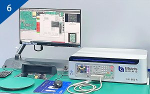
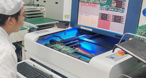
Testing is key to ensuring product compliance. Its purpose is to verify that circuit performance and functionality are normal and to identify potential issues. The process includes AOI (Automated Optical Inspection), ICT (In-Circuit Testing) and FCT (Functional Testing), ensuring that product performance meets design requirements.
6.Packaging and Delivery Stage
The final packaging of the product is completed and the product is delivered to the customer. The purpose is to protect the product and enhance the brand image. The process utilises anti-static packaging and labelling to ensure the product is delivered safely to the customer.
7.Production Schedule
Order acceptance and requirements confirmation take 1 to 2 days, involving the verification of customer requirements, review of the BOM, PCB files and technical specifications. PCB manufacturing takes 5 to 10 days, covering processes such as board processing, etching and drilling; the duration depends on design complexity and production volume. Component procurement takes 3 to 10 days; standard components are usually delivered quickly, but specific components may require additional time, so advance planning is recommended. SMT assembly and DIP insertion take 1 to 3 days; SMT assembly is generally faster, whilst the insertion process varies depending on product complexity. Soldering and assembly take 1 to 2 days to ensure reliable connections between components and the PCB. Testing and inspection take 1 to 3 days, including multiple rounds of testing and defect rectification to ensure the finished product meets specifications. Packaging and dispatch take 1 to 2 days to complete product packaging and arrange logistics for shipment. The total lead time is generally 10 to 20 days, though this may be extended for complex projects or special requirements.
8.Analysis of Quotation Strategy
Pricing principles comprise three aspects. Material costs, including PCB manufacturing and component procurement, account for approximately 60% to 80% of the total cost. Processing fees are calculated based on process complexity and the number of production steps. Testing fees are charged according to the type of test, such as AOI, ICT, and FCT.
There are three billing methods. Pricing by quantity offers discounts for mass production, whilst single-unit samples command higher prices. Pricing by complexity means that higher complexity results in higher processing and testing fees. Transport and packaging costs are calculated based on the delivery method and packaging requirements.
Discount policies include long-term partnership discounts for regular clients. Volume production discounts apply, with unit prices decreasing as order quantities increase. Customised service discounts are available, with additional reductions for clients opting for a full turnkey service.

Conclusion
The full PCBA manufacturing process involves six major stages, with a typical lead time of 10 to 20 days. Quotations must take into account material, manufacturing and testing costs, as well as factors such as quantity and complexity. Understanding the process and quotation mechanism helps clients plan project timelines effectively, optimise cost structures, and achieve the best balance between quality and efficiency.
