
Key Points on Stencil Design and Manufacturing in PCB Assembly
A stencil is the mould used for solder paste printing; the quality of its design directly determines printing accuracy and soldering yield. This article analyses the key parameters and common errors in stencil design to help you optimise the first stage of the SMT process.

Selection of Stencil Material and Thickness
Stencils are typically made from stainless steel (304 or 316) and formed by laser cutting or electroforming.
Thickness Selection: Generally 0.12–0.15 mm for SMT; 0.1–0.12 mm for fine-pitch QFPs; 0.1–0.13 mm for BGAs/CSPs; and 0.15–0.2 mm for high-power components.
Impact of Material: Electroformed stencils have smooth aperture walls and good solder paste release properties, but are costly; laser-cut stencils offer good value for money and are the mainstream choice.

Open Area

The open area ratio is a core parameter in stencil design.
Calculation formula: Open area / Side area of the aperture. Recommended value: ≥0.66 (laser-cut); for electroformed stencils, this may be as low as 0.5.
Significance: An excessively low ratio results in poor solder paste release, leading to insufficient solder or cold joints.
Special Aperture Designs
Aperture shapes must be adjusted for different package types:
BGA: Circular apertures, typically 90–95 per cent of the pad diameter, to prevent bridging.
QFN: Flared or chamfered apertures to improve venting at ground pads.
Large pads: Grid or cross-shaped apertures (Home Plate) to reduce solder paste volume and prevent tombstoning.
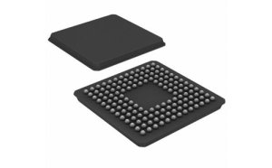
Step Stencil
Used when there are significant differences in component height on the same PCB.
Design considerations: Transitions between thicker areas (e.g. connectors) and thinner areas (e.g. fine-pitch ICs) must be smooth; the step height difference is typically 0.02–0.05 mm; avoid placing steps near fine-pitch components.

Stencil Tension and Service Life
Stencil tension affects printing accuracy.
Standard: New stencils should have a tension of ≥35 N/cm; after some use, ≥30 N/cm.
Service life management: Laser-cut stencils last for approximately 50,000–100,000 prints, whilst electroformed stencils can reach 200,000 prints. Regularly inspect the apertures for wear and burrs on the edges.

Cleaning and Maintenance
Stencil cleaning is key to maintaining print quality.
Cleaning methods: Automatic cleaning machines (water-based or solvent-based), ultrasonic cleaning, and manual wiping.
Frequency: Clean at least once per shift, or inspect after every 5–10 boards printed.
Stencil design is an integral part of DFM. Early communication with stencil engineers at the PCB assembly facility to confirm the aperture layout can significantly reduce first-article defects.
Frequently Asked Questions (FAQ)
Q1: Should the stencil thickness be 0.12 mm or 0.15 mm?
A: This depends on the smallest component package. If there are 0201 components or QFPs with 0.4 mm pitch, select 0.12 mm; if only 0402 components and 0.5 mm pitch are used, 0.15 mm is more cost-effective. For mixed designs, prioritise meeting the finest pitch requirements; high-power areas can be addressed through localised thickening or stepped stencils.
Q2: What is a nano-coating for stencils?
A: A hydrophobic and oleophobic nano-layer is applied to the stencil surface to reduce solder paste residue and improve release properties. The coating has a lifespan of approximately 10,000–20,000 prints and is suitable for fine-pitch and high-density products. Although costs increase by around 20–30 per cent, it reduces cleaning frequency and improves printing yield.
Q3: Why are the stencil apertures smaller than the pads?
A: To prevent excessive solder paste from causing bridging (particularly with BGAs and fine-pitch QFPs). Apertures are typically 85–95 per cent of the pad size. However, ground pads or heat sink pads may require 100 per cent coverage or even an outward extension to ensure sufficient solder volume and venting.
Q4: Can stencils be reused?
A: Yes, but they have a limited lifespan. Laser-cut stencils experience aperture wear after approximately 50,000–100,000 prints, whilst electroformed stencils have a longer lifespan. When storing, they must be laid flat, protected from impact, and kept in a controlled humidity environment to prevent rust. Stencils for different products must not be mixed.
Q5: Does SPI detection identify stencil issues or printing issues?
A: It detects both. When SPI detects anomalies in solder paste volume, this may be due to blocked stencil apertures (requiring cleaning), insufficient stencil tension (requiring replacement), or inappropriate printing parameters (pressure, speed, release angle). Data analysis can help distinguish the root cause.