
HDI PCB Assembly: High-Density Interconnect Manufacturing Explained
Modern electronics demand more function in less space. High-density interconnect, commonly called HDI, is the manufacturing approach that makes this possible. By using microvias, finer traces, and tighter pad pitches, HDI PCB assembly packs far more circuitry into a smaller footprint than conventional board production allows, and it does so without sacrificing the electrical performance that modern devices require.

The technology sits at the heart of smartphones, tablets, wearables, advanced medical instruments, and aerospace electronics. As consumer and industrial products shrink while their capabilities grow, HDI has shifted from a specialized option to a mainstream requirement for competitive hardware design. Engineers who understand its trade-offs can deliver products that simply would not be possible with standard technology.
What Makes a PCB “High-Density Interconnect”
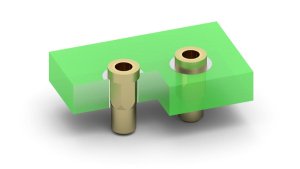
An HDI board is defined by its interconnect density rather than a single material or process. The key differentiator is the microvia: a tiny plated hole, typically under 150 microns in diameter, that connects adjacent layers without consuming the real estate of a traditional through-hole. Because these vias are so small, designers can place them under components and between fine-pitch pads where a mechanical drill could never reach.

Conventional boards rely on drilled through-holes that pass through every layer, limiting routing channels and forcing larger components. HDI replaces many of these with blind vias that reach only outer layers and buried vias hidden entirely inside the stack-up. This frees surface area for components and lets designers route signals on more layers within the same thickness, increasing effective density several times over.
Microvia Formation Methods
Microvias are created with laser drilling rather than mechanical bits. CO2 lasers ablate dielectric materials efficiently and cost-effectively, while UV lasers deliver the precision needed for the smallest diameters and the tightest pad geometries. After drilling, the vias are plated shut to form reliable electrical connections, often with specialized copper deposition to ensure sidewall coverage and prevent voids that would weaken the joint.
Stacked and staggered microvia architectures further increase density. Stacked vias align directly above one another across layers, maximizing vertical routing in a compact zone, while staggered vias offset slightly to improve mechanical reliability by avoiding concentrated stress. Each approach trades manufacturing complexity against routing freedom, and the right choice depends on the signal integrity budget and the fabricator’s proven capabilities.
Typical HDI Stack-Up Structures
HDI constructions are classified by how many build-up layers they use. A 1+N+1 stack-up has one microvia layer on each side of a core, while 2+N+2 adds a second build-up on each side. Higher orders such as 3+N+3 or any-layer interconnect support the densest designs found in flagship mobile devices, where every cubic millimeter is contested by batteries, cameras, and antennas.
The core itself may be a standard FR-4, but the build-up layers often use newer resin systems with lower dielectric loss and tighter dimensional stability. This combination preserves signal speed while keeping cost manageable for volume production, and it allows RF and digital functions to coexist in a single compact assembly rather than requiring separate boards.
Material Considerations
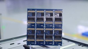
Because traces are finer and spaces tighter, HDI demands tighter registration and cleaner etching than standard boards. Low-profile copper foils and flat dielectric surfaces reduce the risk of open circuits at fine pitches, while controlled-impedance materials keep high-speed signals intact. A qualified PCB assembly manufacturerhelps select materials that balance performance, yield, and budget for each project, avoiding the common trap of over-specifying expensive laminates where simpler ones would suffice.
Assembly Challenges Unique to HDI
HDI boards present specific assembly hurdles that standard lines may not handle well. Components such as chip-scale packages, ball-grid arrays, and passives in 0201 or 01005 sizes sit on pads only fractions of a millimeter wide. Pick-and-place machines must hold tighter placement accuracy, and reflow profiles need tuning to avoid damaging thin dielectric layers or causing pad cratering during thermal cycling.
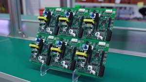
Warpage becomes a real concern because thin, asymmetric stacks behave differently under thermal load. Boards that bow during reflow lose paste contact and produce defective joints. Careful panel design, symmetric copper distribution, and compatible lamination profiles keep warpage within acceptable limits throughout the thermal cycle, and the panel itself provides mechanical support that counters the tendency.
Inspection Requirements
X-ray inspection becomes essential because the smallest joints are invisible to optical systems. Automated optical inspection still covers exposed features, but buried connections and hidden BGA spheres require X-ray to confirm solder volume, voiding, and bridging. Building inspection strategy into the process plan prevents escaped defects and reduces costly field returns that damage customer trust.
Design Rules That Protect Yield
Successful HDI assembly starts with design for manufacturing. Pad sizes should match component terminals closely, annular rings must meet fabricator capabilities, and microvia aspect ratios should stay within proven limits. Over-aggressive designs that exceed these limits simply will not yield at volume, no matter how capable the line appears on paper, and they generate expensive engineering change orders.
Thermal management also matters. Dense layouts concentrate heat, so embedded thermal vias and careful copper distribution keep junction temperatures in range. Early simulation of both electrical and thermal behavior prevents costly re-spins later, and it is far cheaper to validate a design virtually than to discover a flaw after the first prototype build has already consumed schedule.
Engineers exploring dense layouts should discuss stack-up options with a one-stop PCBA solution before finalizing the schematic. The right early decisions save weeks of iteration and protect production margins, while late changes to via strategy can force an entirely new fabrication setup and requalification.
Cost Drivers and Trade-Offs
HDI costs more than standard PCBs, driven by laser drilling, additional lamination cycles, and tighter process control. However, the savings from smaller boards, fewer layers in some cases, and higher functional density often offset the premium at the system level. The economic case strengthens as device miniaturization becomes a market requirement rather than a differentiator that only premium products pursue.
Choosing the lowest viable HDI order keeps cost down without giving up necessary performance. Not every design needs any-layer interconnect; many products are perfectly served by a 1+N+1 or 2+N+2 structure that balances capability and price, and stepping down an order can cut cost significantly with no functional penalty.
HDI Design Checklist
Before releasing an HDI design, verify that via diameters and pad sizes match the fabricator’s published capabilities, that microvia aspect ratios stay within limits, that thermal vias are placed under high-power devices, and that impedance-controlled traces have documented targets. Confirm that the stack-up drawing lists every material and thickness, and that the panel plan keeps components clear of break lines.
A short design-review meeting with the assembly partner before fabrication catches most issues while they are still cheap to fix. This single step routinely prevents the majority of production surprises and protects both schedule and yield.
Future Trends in HDI
The technology continues to advance. Embedded components placed inside the build-up layers free even more surface area, and newer substrate-like materials blur the line between package and board. As wearable and medical devices push size limits further, HDI will keep evolving toward finer features and higher layer counts without sacrificing reliability.
The trend toward miniaturization means HDI adoption keeps climbing across industries. Designers who understand its trade-offs position their products to meet tomorrow’s packaging demands without compromise, and they avoid the expensive surprises that come from treating HDI as an afterthought rather than a planned strategy.