

No single test method catches every defect in PCB assembly. Each technique covers different failure modes, operates at different points in the production flow, and comes with different cost and cycle time implications. An effective test strategy combines multiple methods, positioned where they provide maximum defect detection value at minimum cost and throughput impact.
This article examines the major test methods used in PCB assembly, their capabilities and limitations, and how to combine them into a test strategy tailored to your product and production volume.
Automated Optical Inspection: The First Quality Gate
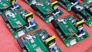
Automated optical inspection uses high-resolution cameras and image processing to inspect solder joints and component placement after reflow. Modern AOI systems capture multiple images of each inspection target from different angles, using variable lighting to highlight specific solder joint characteristics. The system compares each target against programmed acceptance criteria and flags anomalies for operator review.
AOI is effective at detecting visual defects including missing components, wrong component polarity, solder bridges, insufficient solder, excess solder, component misalignment, and tombstoning. It operates at production line speed, inspecting each board in seconds without slowing throughput. This makes AOI the primary in-line inspection method for most SMT assembly operations.
The limitation of AOI is that it can only inspect what it can see. Hidden solder joints under BGA packages, QFN thermal pads, and shielded components are invisible to optical inspection. AOI also struggles with solder joint quality inside partially visible joints, such as J-leaded components where the critical solder fillet is partially obscured. For these hidden joints, X-ray inspection is required.
AOI programming quality is the single largest determinant of inspection effectiveness. A well-programmed system achieves high defect detection rates with low false alarm rates. A poorly programmed system either misses defects or generates excessive false calls that consume operator review time. Programming should be validated during pilot production by intentionally introducing known defects and verifying the system detects them. The program should be updated based on production defect data to catch newly discovered failure modes.
Pre-Reflow and Post-Placement AOI
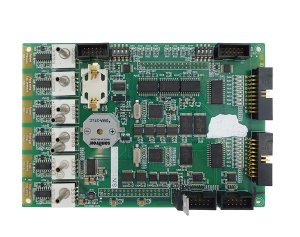
Some production lines include AOI after component placement but before reflow. This pre-reflow inspection catches placement errors while they are still easy to correct. A misplaced component on solder paste can be removed and re-placed without desoldering. After reflow, the same correction requires desoldering, which is slower and risks board damage.
Pre-reflow AOI is particularly valuable for first-article builds, high-mix production where changeover frequency increases setup error risk, and assemblies with high component counts where the probability of a placement error increases. The investment in an additional AOI station must be justified by the reduction in rework cost and cycle time for placement defects.
X-Ray Inspection: Seeing the Invisible
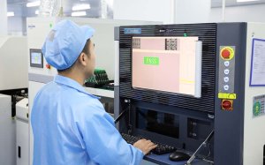
X-ray inspection penetrates component bodies and board materials to reveal hidden solder joints. For BGA assemblies, X-ray is the only practical method for verifying joint quality in production. It also reveals voiding levels, ball shape and uniformity, and bridging beneath component packages that optical inspection cannot detect.
Two-dimensional X-ray systems provide a top-down view of the joint array, suitable for detecting gross defects like missing balls, large voids, and bridging. Three-dimensional X-ray, using computed tomography or laminography, slices through the joint at different heights, providing detailed information about void distribution, pad wetting, and joint geometry. For high-reliability applications, 3D X-ray is becoming the standard.
X-ray inspection is slower than AOI, requiring more time per board. For this reason, 100 percent X-ray inspection is typically reserved for products with BGA components or high-reliability requirements. For other products, sampling X-ray inspection may be used to monitor process health without inspecting every board. The sampling rate should be determined based on the defect risk and the cost of escaping defects to downstream testing or customers.
In-Circuit Testing: Comprehensive Electrical Verification
In-circuit testing uses a bed-of-nails fixture to access individual circuit nodes and verify component values, short circuits, open circuits, and basic functionality. The test fixture contains spring-loaded pins that contact test points on the board, allowing the test system to measure each component in isolation from its neighbors.
ICT is powerful because it can detect defects that visual inspection and functional testing miss. A wrong-value resistor, a shorted capacitor, an open inductor: these component-level defects may not cause functional test failures but indicate a process or material issue that needs correction. ICT catches these defects at the component level, enabling precise root cause analysis.
The fixture is the primary limitation of ICT. Each board design requires a custom fixture, which costs several thousand dollars and takes weeks to fabricate. This makes ICT most cost-effective for higher-volume products where the fixture cost is amortized across many boards. For low-volume or frequently changing products, the fixture cost and lead time may not be justified.
ICT also requires test points on the board, which consume area and may affect routing density. The trend toward higher component density and smaller board areas makes it increasingly difficult to allocate test points for every node. Designers must balance test access requirements against density goals, and the test strategy must account for nodes that cannot be accessed.
Flying Probe Testing: Fixtureless Flexibility
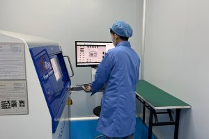
Flying probe testing provides ICT-like electrical verification without a custom fixture. The system uses movable probes that navigate to test points on the board, contacting them one at a time to perform measurements. Multiple probes operate simultaneously, with the system optimizing the probe movement sequence for efficiency.
The primary advantage of flying probe testing is flexibility. A new board design can be tested with only programming changes, no fixture fabrication. This makes flying probe ideal for prototyping, low-volume production, and high-mix environments where fixture costs would be prohibitive. The test can be ready within hours of receiving the board design, compared to weeks for ICT fixture fabrication.
The tradeoff is speed. Flying probe testing is significantly slower than ICT because each measurement requires the probe to move to the test point position. A test that takes seconds on an ICT fixture may take minutes on a flying probe system. For high-volume production, this cycle time penalty makes flying probe impractical unless supplemented by ICT for volume runs.
Flying probe also requires test points, though it can sometimes access component pads or vias that ICT fixtures cannot reach due to fixture pin geometry constraints. The flexibility in probe positioning allows testing of boards with limited dedicated test points, though coverage may be incomplete compared to a purpose-designed ICT fixture.
Functional Testing: Does the Product Work?
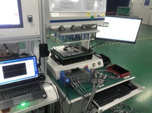
Functional testing exercises the assembled board as a complete system, verifying that it performs its intended function. Unlike ICT, which tests individual components, functional test verifies that the circuit works correctly as a whole. This catches integration defects that component-level testing may miss, such as timing issues, signal integrity problems, and software-hardware interaction failures.
Functional test development requires defining the test cases that exercise the product’s features, designing the test fixture that interfaces the board to the test system, and developing the test software that executes the test sequence and reports results. This development effort is significant but amortized across the product’s production life.
The challenge with functional testing is fault isolation. When a functional test fails, the failure may be caused by any of hundreds of components or connections. Diagnosing the root cause can be time-consuming, particularly for intermittent failures. For this reason, functional testing is most effective when preceded by component-level testing that catches the majority of defects before functional test.
Boundary scan testing, based on JTAG interfaces, provides a middle ground between component-level and functional testing. Boundary scan tests the interconnections between compliant devices without physical test point access. This is particularly valuable for high-density boards where physical test points are scarce. However, boundary scan only works with devices that include boundary scan logic, and coverage is limited to interconnections between compliant devices.
Building a Test Strategy
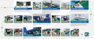
An effective test strategy layers methods to achieve appropriate coverage at acceptable cost. For a typical SMT assembly, the strategy might include solder paste inspection at 100 percent after printing, AOI at 100 percent after reflow, X-ray inspection at 100 percent for BGA assemblies or sampling for non-BGA, ICT at 100 percent for volume production or flying probe for low volume, and functional test at 100 percent before shipment.
The specific strategy should be tailored to the product’s risk profile, production volume, and cost constraints. High-reliability products warrant more comprehensive testing, with 100 percent coverage at multiple stages. Consumer products may use sampling for some test methods to control cost. And products with design changes or new component introductions should receive enhanced testing until the process is proven stable.
The test strategy should be documented in a test plan that defines what is tested, how it is tested, what the pass/fail criteria are, and what happens to failures. The plan should be reviewed and updated based on production data, adding tests for newly discovered failure modes and removing tests that never find defects. A PCB assembly manufacturer with comprehensive test capabilities and experienced test engineering support can help develop a strategy that optimizes coverage and cost for your specific product. A full-service PCBA partner should offer AOI, X-ray, ICT, flying probe, and functional testing, allowing the optimal combination for each assembly type.
