
Assembly Processes for High-Frequency/RF PCBs
High-frequency and radio frequency (RF) PCBs are widely used in 5G communications, radar, satellites, and test equipment. Their assembly processes place extremely high demands on signal integrity, impedance control, and cleanliness. This article analyzes the key technologies involved in high-frequency PCB assembly.
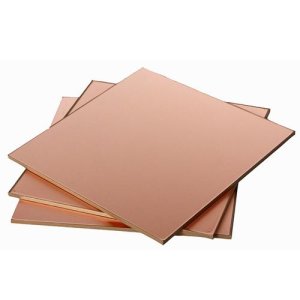
Characteristics of High-Frequency PCB Materials
High-frequency PCBs use specialized substrates, with dielectric constant (Dk) and loss factor (Df) serving as key performance indicators.
Common materials include Rogers RO4350B, Taconic TLY-5, Isola I-Tera MT40, and PTFE (polytetrafluoroethylene).
Differences from FR-4: Better Dk stability (minimal variation with temperature/frequency), lower Df (less signal loss), but 5–20 times higher cost and greater processing difficulty (PTFE is soft and has a high coefficient of thermal expansion).
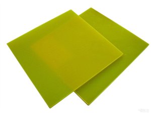
Impedance Control Accuracy
RF signals are sensitive to impedance matching; reflections can cause signal distortion.
Control Requirements: Impedance tolerance is typically ±5% (compared to ±10% for standard boards). Precise control of trace width, copper thickness, dielectric thickness, and Dk values is required.
Verification Methods: TDR (Time-Domain Reflectometer) testing and S-parameter measurements using a vector network analyzer (VNA).
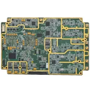
Surface Finish Options
The surface finish of high-frequency boards affects signal transmission and reliability.
Recommended Options: Electroless nickel-gold (ENIG; good flatness but high skin effect loss), electroless tin (low cost but short shelf life), and electroless silver (good conductivity but prone to sulfidation).
Options to Avoid: HASL (hot air leveling; surface irregularities cause impedance discontinuities) and OSP (poor stability at high frequencies).
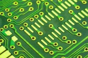
SMT Process Adjustments
High-frequency components (such as RF connectors, filters, and power amplifier chips) are process-sensitive.
Placement Accuracy: RF connector pins require high coplanarity with ground pads; placement offset can cause sudden impedance changes.
Reflow Parameters: High-frequency board materials have low Tg (especially PTFE); peak temperature must be reduced and high-temperature exposure time shortened to prevent substrate warping.
Cleanliness Requirements
High-frequency signals are sensitive to residues.
Cleaning Standards: Ion contamination < 0.5 μg NaCl eq/cm² (stricter than for standard boards) and no visible flux residue.
Cleaning Methods: Solvent cleaning or vapor-phase cleaning to avoid residual ions from water-based cleaning.
Shielding and Grounding
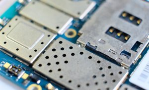
RF boards require a comprehensive shielding and grounding design.
Assembly Key Points: Soldering of shielding covers (to ensure ground continuity), dense arrays of ground vias, and grounding of RF connector housings.
Testing and Verification: Measure S11 (reflection coefficient) and S21 (transmission coefficient) using a network analyzer to verify shielding effectiveness.
High-frequency board assembly is a precision process. Select a PCB assembly factory with experience in RF products and confirm that it possesses the capabilities for high-frequency board processing, precision impedance testing, and RF debugging.
Frequently Asked Questions (FAQ)
Q1: Why can’t standard FR-4 be used for high-frequency boards?
A: The Dk and Df of FR-4 deteriorate significantly as frequency increases, leading to severe signal attenuation and distortion. At frequencies above 1 GHz, FR-4’s Df is approximately 0.02, whereas Rogers RO4350B has a Df of only 0.0037, reducing loss by more than five times. Dedicated high-frequency materials must be used for 5G millimeter-wave applications (>24 GHz).
Q2: Why is ENIG surface treatment not suitable for all high-frequency applications?
A: The nickel layer in ENIG causes skin effect loss, which increases with higher frequencies. For applications above 10 GHz, electroless silver plating or OSP is recommended (though OSP has a short shelf life). Alternatively, selective surface treatment can be used: electroless silver plating for RF areas and ENIG for other areas.
Q3: What are the special requirements for soldering RF connectors?
A: The ground pins of RF connectors (such as SMA and MMCX) must be connected to the PCB ground plane with low impedance. Requirements: 1) Ground pads must have a large copper area; 2) Dense ground vias (spacing < 1 mm); 3) Ground pins must be fully wetted during soldering; 4) Coplanarity < 0.1 mm to prevent impedance discontinuities.
Q4: How is microstrip line impedance tested on high-frequency boards?
A: During production: Create a test coupon at the edge of the PCB and measure using a TDR or VNA. For finished products: Measure directly at test points or connectors on the product. Note: Probe contact introduces parasitic capacitance, which requires calibration or de-embedding.
Q5: Why is PTFE sheet material difficult to process?
A: PTFE (polytetrafluoroethylene) is soft, has a high coefficient of thermal expansion, and has poor adhesion to copper foil. It is prone to burrs during drilling, slippage during lamination, and warping during reflow soldering. Specialized equipment and processes are required: low-temperature lamination, plasma treatment to enhance adhesion, and low-stress SMT fixtures.