

Reviewing PCB designs prior to SMT assembly is a crucial step in ensuring smooth production and product quality. This article provides a detailed explanation of the five key review processes: receipt and data verification, design specification review, manufacturability assessment, confirmation of key parameters, and component layout evaluation. It also offers solutions for five key technical aspects: pad design, via placement, component polarity, board warpage, and component density.

1.Receipt and Data Verification
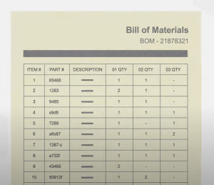
Upon receiving the client’s PCB files—including Gerber files, BOMs and coordinate files—the SMT manufacturer’s first step is to verify these documents. It is essential to ensure the completeness and accuracy of the files; in particular, the BOM must correspond precisely with the coordinate files to prevent components from being omitted or incorrectly placed.
2.Design Specification Review
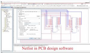
The PCB design is reviewed to ensure it complies with SMT manufacturing process requirements. For example, checks are made to confirm that pad sizes, spacing, and via diameters meet component placement requirements; that there is sufficient space in the soldering areas; and that there are no irregular shapes that might affect soldering quality.
3. Manufacturability Check
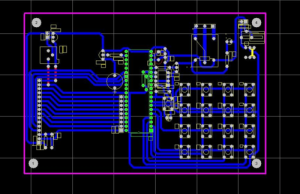
The PCB design is reviewed from a production perspective to ensure it is feasible given existing manufacturing capabilities. Attention must be paid to minimum pad sizes, minimum component spacing, and the positional relationship between vias and pads. This step prevents components from being incorrectly placed or soldered during production due to an ill-conceived design.
4.Confirmation of Key Parameters
In SMT assembly, solder paste thickness, temperature profiles and reflow soldering parameters are key factors that directly affect soldering quality. It is necessary to confirm the PCB material, thickness, copper foil thickness and whether it is a multilayer board; these factors will determine the soldering process to be used and the corresponding type of solder paste.
5.Assessment of Component Layout Rationality
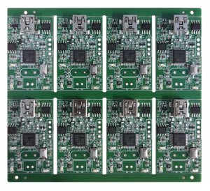
The focus is on checking the component layout to ensure it is reasonable, avoids high-temperature areas, prevents heat dissipation issues caused by component density, and takes into account the convenience of subsequent testing and debugging. This not only affects production efficiency but is also directly related to the reliability of the final product.
6.Key Points of Land Design
The design of the lands directly determines the quality of component soldering. It is essential to ensure that the pad size matches the component lead dimensions; pads that are too small will result in an unstable solder joint, whilst those that are too large may cause bridging or cold solder joints. Common issues also include pads not being treated with a solder mask, leading to short circuits between adjacent pads.

The solution is to select appropriate pad dimensions during the design phase, adhering to the pad design recommendations set out in the industry standard IPC-7351. Manufacturers can provide DFM recommendations based on customer requirements to optimise pad design.
7. Relationship between Via and Pad Position
When vias are positioned close to pads, solder paste is likely to flow into the vias, causing cold solder joints or porosity issues. This is particularly likely to occur around high-density components such as Ball Grid Arrays (BGAs).
The solution is to ensure sufficient spacing between vias and pads during the design phase, or to use a process involving a solder mask to prevent solder paste from flowing in.
8. Verification of Component Polarity and Orientation
In SMT assembly, incorrect orientation of polarised components such as capacitors, inductors and diodes is a common issue. If polarity markings in the PCB design are unclear or incorrect, this will significantly increase the likelihood of rework.
The solution is to ensure that polarised components have clear polarity markings in the PCB design, and to carry out multiple checks against the BOM and coordinate files prior to assembly, conducting a double-check to ensure the correct component orientation.
9.PCB Warpage Control
PCB warpage affects the flatness of component soldering; particularly during the reflow soldering process, excessive warpage may lead to solder joint failure or component damage.
The solution is to select PCB materials of appropriate thickness and to lay out large-volume components reasonably in the design to reduce stress, whilst implementing strict warpage control standards to guarantee the final product quality.
10.Component Density and Thermal Management
High-density component layouts are prone to uneven heat dissipation during the soldering process, leading to localised overheating or poor soldering. At the same time, particular attention must be paid to the temperature distribution around high-power components to prevent damage caused by excessive heat.
The solution is to allow for adequate heat dissipation space in the design; where necessary, incorporate ventilation holes or employ techniques such as thickened copper foil, whilst utilising precise temperature control technologies in high-density component designs.

11.Common Issues and Solutions
Solder bridging: Resolved by adjusting the solder paste thickness or optimising the stencil aperture design.
Component misalignment or displacement: Utilise advanced AOI (Automated Optical Inspection) equipment to perform precise positioning checks at every stage, ensuring each component is correctly positioned.
Cold solder joints or poor solder joints: Optimise the reflow soldering temperature profile and use high-quality solder paste to ensure strong and reliable solder joints.
Conclusion
PCB design review prior to SMT assembly is the first line of defence in preventing production defects and safeguarding product quality. By implementing a systematic review process and controlling key technical aspects, potential design issues are eliminated at source, ensuring the smooth execution of subsequent assembly, soldering and testing stages. This forms the fundamental guarantee for the efficient and high-quality delivery of PCBA products.
