
Lead-free soldering has become the mainstream trend in electronics manufacturing, but leaded processes are still used in specific sectors. This article examines the technical differences, cost implications and suitable applications of these two processes in PCB assembly to help you make the right choice.
Driven by Environmental Regulations
The RoHS Directive restricts the use of hazardous substances such as lead and has been mandatorily implemented in the European Union, China, and California, USA, amongst other regions. Exported products must comply with lead-free standards.
Key regulatory points: maximum lead content of 0.1 per cent, labelling requirements, and compliance documentation.
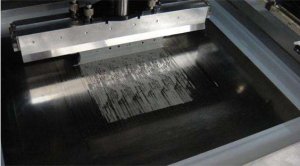
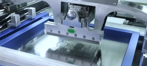
Differences in Solder Paste Materials
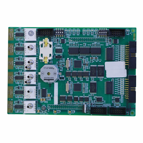
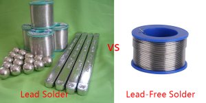
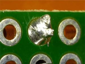
Leaded solder paste (Sn63Pb37) has a melting point of 183°C, offers good wettability, and produces bright solder joints. Lead-free solder paste (SAC305) has a melting point of 217–219°C, poorer wettability and produces matt solder joints.
Impact of materials: Lead-free solder paste is 20–30% more expensive, requires higher flux activity and has stricter storage conditions.
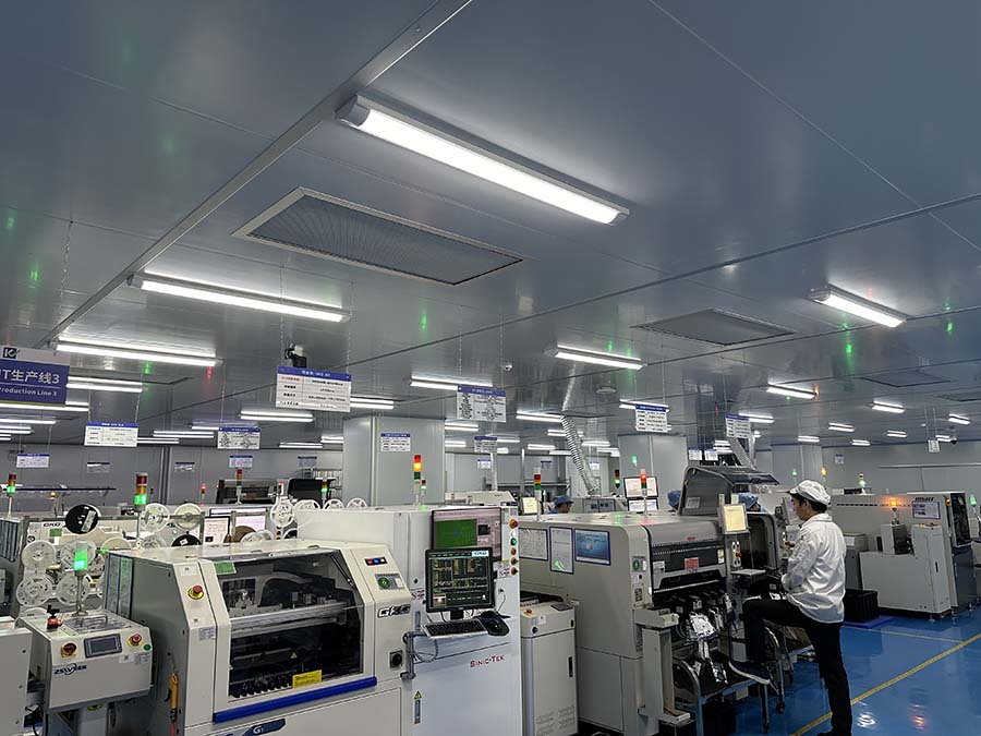
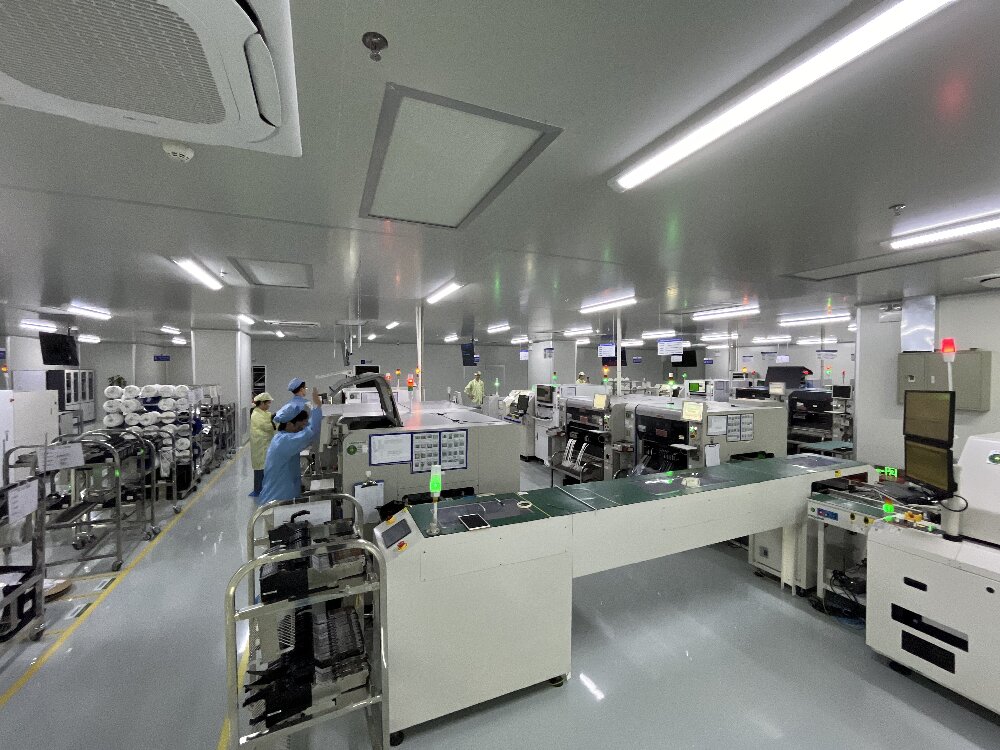
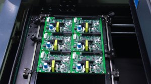
Equipment and Process Adjustments
Lead-free processes require higher reflow temperatures, placing new demands on equipment.
Key adjustments: upgrading the highest temperature zone of the reflow oven; using nitrogen protection to reduce oxidation; selecting high-temperature-resistant board materials (e.g. high Tg FR-4).
Comparison of Solder Joint Reliability
Leaded solder joints offer good ductility and excellent fatigue resistance. Lead-free solder joints are harder, but the risks of tin whisker growth and electromigration must be monitored.
Long-term reliability: Lead-free solder joints perform more consistently in high-temperature, high-humidity environments; tin whisker issues can be mitigated through plating processes.
Cost Analysis
The direct costs of lead-free processes are higher; however, total costs must take into account environmental compliance and export restrictions.
Cost components: Solder paste premium, increased energy consumption, equipment upgrades, and certification fees.
Recommended Applications
Leaded Process: Specially exempted sectors such as defence and aerospace; high-reliability analogue circuits; cost-sensitive consumer electronics (non-export).
Lead-free Process: Exported consumer electronics; medical electronics; automotive electronics; general industrial control.
When selecting a process, regulatory requirements, product positioning and supply chain capabilities must be considered comprehensively. Confirm the PCB assembly factory’s lead-free process certification and practical experience.
Frequently Asked Questions (FAQ)
Q1: Why do lead-free solder joints appear duller?
A: The alloy composition of lead-free solder paste (SAC305) results in a higher surface roughness on the solder joints, giving them a matt appearance. This is normal and does not indicate poor soldering quality. The IPC-A-610 standard explicitly accepts the matt appearance of lead-free solder joints.
Q2: By how much does the lead-free process increase costs?
A: The solder paste itself is 20–30% more expensive. Combined with increased energy consumption (reflow temperatures are 20–30°C higher) and potential equipment upgrades, the overall manufacturing cost increases by approximately 10–15%. However, this avoids the risk of environmental compliance breaches and export restrictions.
Q3: Can leaded and lead-free products be manufactured on the same production line?
A: Yes, but strict segregation is required. Stencils, squeegees and reflow ovens must be thoroughly cleaned to prevent cross-contamination. It is recommended to produce them at different times or on separate production lines to minimise the risk of material mix-ups.
Q4: What are tin whiskers?
A: These are needle-like crystals that form naturally on the surface of pure tin or high-tin alloys and may cause short circuits. The risk of tin whiskers is lower with SAC305 alloys than with pure tin plating and can be suppressed through annealing or by adding elements such as bismuth or antimony.
Q5: Are there any special requirements for PCB laminates in lead-free processes?
A: Yes. Lead-free reflow temperatures are higher and require laminates with a high Tg (glass transition temperature), typically Tg ≥ 150°C. Standard FR-4 (Tg 130–140°C) may delaminate or warp at high lead-free reflow temperatures.