
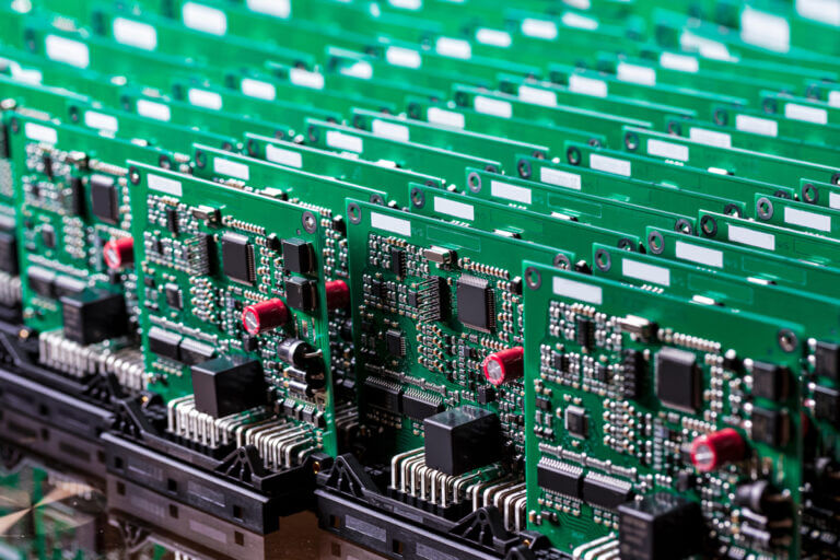
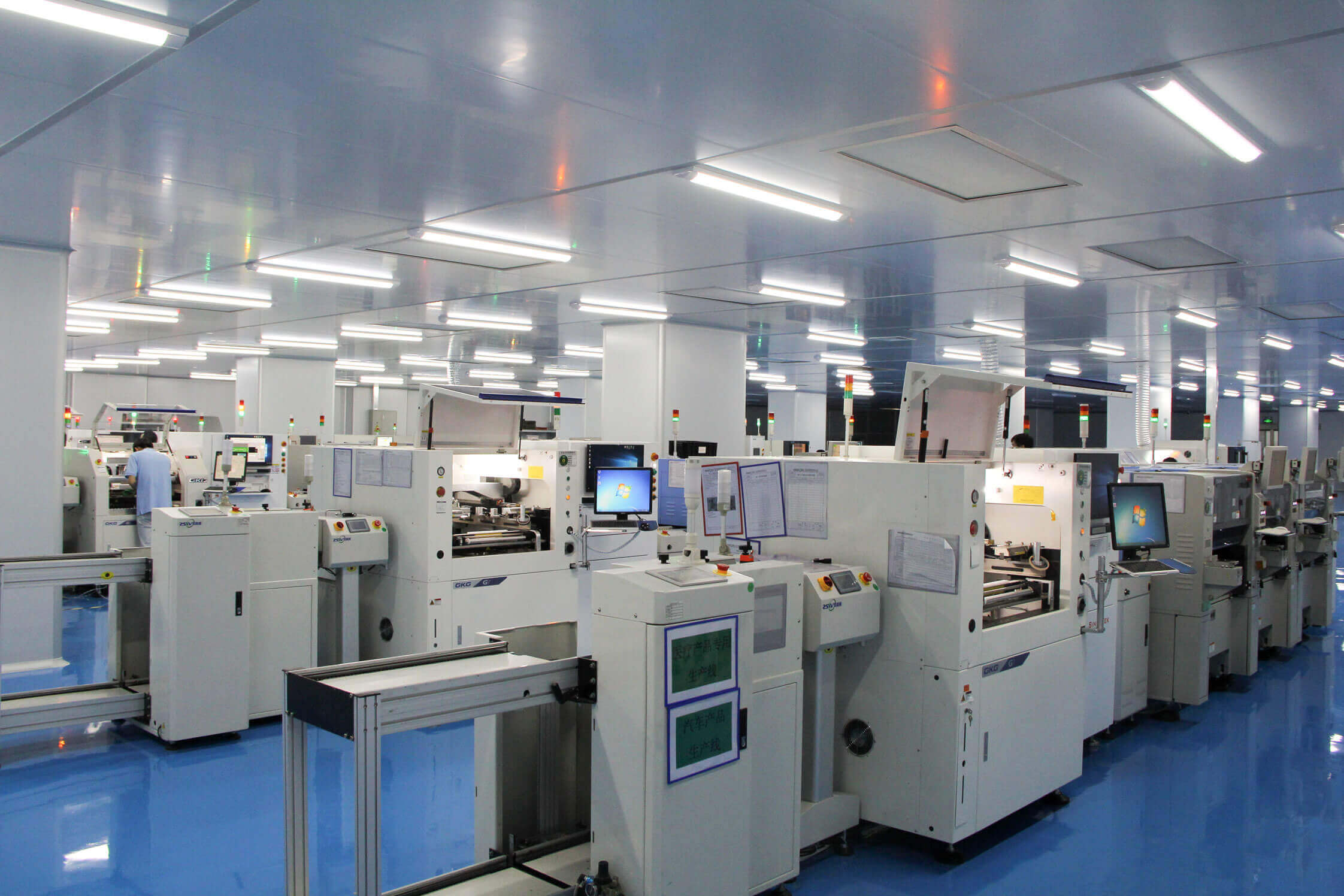
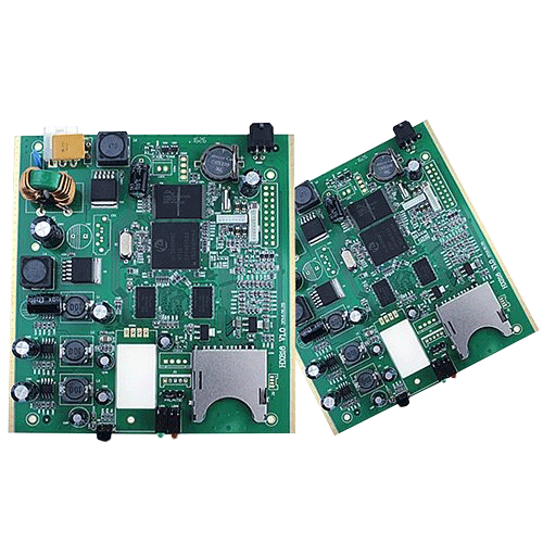
BGA (Ball Grid Array) soldering is one of the most challenging processes in PCB assembly. As the solder joints are concealed beneath the package and cannot be visually inspected, this process places extremely high demands on equipment and process control. This article analyses the key technical aspects of BGA soldering to help you understand this complex process.

Characteristics of BGA Packages and Soldering Challenges
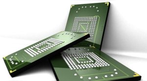
BGAs connect to PCB pads via solder balls on their underside, offering high pin density and excellent electrical performance. However, the concealed solder joints make inspection difficult, and improper temperature control during reflow soldering can easily lead to voids and bridging.
Main challenges: invisible solder joints, strict requirements for coefficient of thermal expansion (CTE) matching, and high difficulty in rework.
Stencil Aperture Design
Stencil apertures directly affect the amount of solder paste applied. The aperture area ratio (aperture area divided by pad area) is typically controlled between 0.55 and 0.75.
Design considerations: Circular apertures are preferable to square ones; avoid excessively large apertures to prevent solder balls; for thick boards, consider using a stepped stencil.
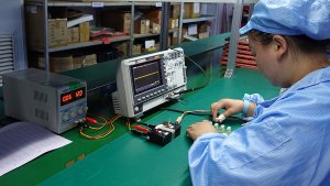
Reflow Soldering Temperature Profile
BGAs are sensitive to temperature profiles. During the preheating stage, the heating rate should be controlled at 1–2 °C/second to prevent thermal shock.
Key parameters: peak temperature 235–245 °C; time spent above the liquidus 60–90 seconds; cooling rate not exceeding 4 °C/second.
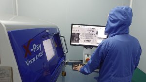
X-ray inspection standards
X-ray is the primary method for inspecting BGA solder joints. Two-dimensional X-ray can detect bridging, misalignment and voids, whilst three-dimensional CT scanning can analyse the shape of the solder joints.
Acceptance criteria: Void rate not exceeding 25 per cent; no bridging; no ‘head-in-pillow’ effect.
Rework Process Control
BGA rework requires the use of a dedicated rework station, with localised heating to avoid affecting surrounding components.
Rework procedure: Preheating and removal, pad cleaning, re-balling or applying solder paste, precision placement, reflow soldering.
Analysis of Common Defects
Pillow effect: Caused by oxidation of solder balls or insufficient reflow. Countermeasures: Control the reflow atmosphere and optimise the temperature profile.
Excessive voids: Caused by poor pad plating or residual solder paste flux. Countermeasures: Improve PCB surface treatment and select low-void solder paste.
Understanding the BGA soldering process helps to mitigate risks during the design phase. Maintain close communication with the PCB assembly factory to ensure it possesses the necessary BGA processing and inspection capabilities.
Frequently Asked Questions (FAQ)
Q1: Why is BGA soldering more difficult than standard SMT?
A: BGA solder joints are hidden beneath the package and cannot be inspected visually; X-ray or CT inspection is required. Furthermore, the small spacing between solder balls (e.g. 0.4 mm) places higher demands on placement accuracy and reflow temperature control.
Q2: What is the acceptable void rate for BGAs?
A: The general industry standard is that individual voids must not exceed 25 per cent, and the total void area must not exceed 30 per cent. However, sectors with high standards, such as aerospace and medical applications, have stricter requirements and may require a rate of less than 10 per cent.
Q3: Can BGAs be soldered by hand?
A: This is not recommended. BGAs require precise temperature profiles and uniform heating, which cannot be controlled using a hand-held hot-air gun. A reflow oven or a dedicated BGA rework station must be used.
Q4: What is the ‘Head-in-Pillow’ effect?
A: This refers to a situation where the solder ball and pad have not fully fused, resulting in a layered structure resembling a pillow. Causes include oxidation of the solder ball, insufficient reflow temperature or flux failure. A distinct boundary line is visible under X-ray.
Q5: Can BGA rework damage the PCB?
A: There is a risk. Repeated rework may lead to pad detachment or PCB delamination. It is recommended to limit rework to no more than two attempts and to use bottom preheating to reduce thermal stress.