

What is PCB Fabrication vs PCBA Assembly?
Many hardware teams use the terms PCB and PCBA interchangeably, but they represent fundamentally different stages of electronics manufacturing. A PCB is a bare substrate with copper traces and drilled holes. A PCBA is a functional electronic assembly with components soldered to that substrate. Understanding the distinction — and the relationship between the two processes — is essential for project planning, supplier selection, and cost management. At Keepbest, we manage both fabrication coordination and assembly in-house, giving customers a single point of accountability from bare board to finished product.
What Is PCB Fabrication?
PCB fabrication transforms a design file into a physical bare board. It is a subtractive and additive manufacturing process that creates the electrical interconnect structure on which components will later be mounted.
The Fabrication Process:
Inner Layer Processing: For multilayer boards, copper foil is laminated onto thin FR-4 cores. Photoresist is applied, exposed to the inner layer artwork, and developed. Unwanted copper is etched away, leaving the desired trace pattern.
Layer Lamination: Inner layers, prepreg (partially cured resin), and copper foil are stacked in a press under heat and pressure. The prepreg flows and cures, bonding the layers into a solid panel.
Drilling: Through holes, blind vias, and buried vias are drilled with high-speed mechanical drills or lasers. Hole position accuracy is critical for subsequent plating and alignment.
Plating: A thin layer of copper is electrolessly deposited on hole walls and board surfaces. Additional electrolytic copper is plated to achieve the required barrel thickness, typically 20-25 microns for standard applications.
Outer Layer Processing: Photoresist, exposure, and etching define the outer layer traces. Surface finish is applied — typically ENIG, HASL, OSP, or immersion tin depending on shelf life, solderability, and cost requirements.
Electrical Test: A flying-probe or bed-of-nails tester verifies that every net is continuous and isolated from every other net. This catches fabrication defects before the board reaches assembly.
Routing and Inspection: Panels are routed into individual boards. Dimensional inspection, AOI for trace quality, and final cleaning complete the process.
| Fabrication Parameter | Typical Specification | Impact on Assembly |
| Layer count | 2-24+ layers | Higher layer count increases cost and fabrication time; may affect reflow warpage |
| Minimum trace/space | 75 microns / 75 microns | Finer traces require more precise assembly alignment |
| Surface finish | ENIG / HASL / OSP | ENIG preferred for long shelf life; OSP for cost-sensitive quick-turn |
| Impedance control | Plus or minus 5-10% | Critical for high-speed designs; requires fabrication process control |
| Via types | Through, blind, buried, microvia | Hidden vias require X-ray inspection during assembly |
What Is PCBA Assembly?
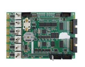
PCBA assembly mounts and solder electronic components onto the fabricated bare board. It transforms the passive substrate into an active, functional electronic device.
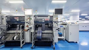
The Assembly Process:
Solder Paste Printing: Solder paste is deposited through a laser-cut stencil onto every pad that will receive a surface-mount component.
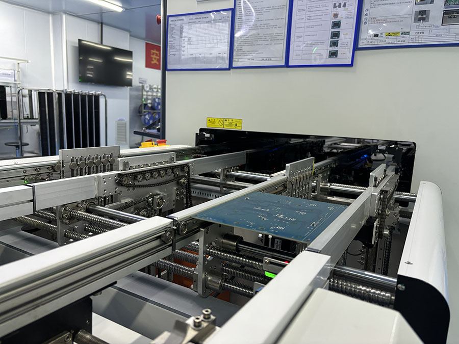
Component Placement: Pick-and-place machines retrieve components from tape-and-reel feeders and position them on the paste deposits with micron-level accuracy.
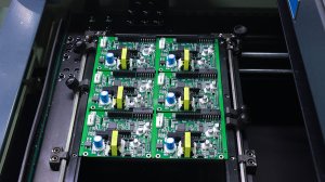
Reflow Soldering: The populated board passes through a multi-zone oven where the temperature profile melts solder paste and forms permanent metallurgical joints.
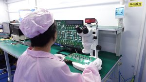
Inspection: SPI verifies paste quality. AOI detects placement and solder defects. X-ray inspects hidden joints under BGAs and QFNs.
Through-Hole Processing: If required, through-hole components are inserted and soldered via wave or selective soldering.
Testing: ICT verifies electrical parameters. FCT validates functional performance under operating conditions.
| Assembly Stage | Key Equipment | Quality Output |
| Paste printing | Stencil printer + SPI | Consistent paste volume per pad |
| Placement | Pick-and-place machine | Accurate component position and orientation |
| Reflow | Multi-zone nitrogen oven | Reliable solder joints with minimal voids |
| Inspection | AOI + X-ray | Defect detection before shipment |
| Test | ICT + FCT | Electrical and functional validation |
Key Differences Between Fabrication and Assembly
| Attribute | PCB Fabrication | PCBA Assembly |
| Raw material | Copper clad laminate, prepreg, foil | Components, solder paste, flux |
| Core process | Etching, drilling, plating, lamination | Printing, placement, soldering, testing |
| Capital equipment | Drillers, laminators, plating lines, etchers | Printers, pick-and-place, reflow ovens, testers |
| Skill requirement | Chemical process engineering | Precision mechanical and electrical assembly |
| Defect types | Shorts, opens, delamination, impedance deviation | Bridging, tombstoning, voids, misalignment |
| Lead time | 5-15 days for standard boards | 2-5 weeks including component procurement |
| NRE components | Panel tooling, drill programs, test fixtures | Stencils, placement programs, test fixtures |
Why the Distinction Matters for Procurement
Supplier Specialization: Some manufacturers specialize in fabrication only. Others specialize in assembly only. A few offer both. Understanding which capability you need prevents mismatched expectations.
Schedule Coordination: Fabrication must complete before assembly can begin. However, component procurement (for assembly) and stencil fabrication can run in parallel with PCB manufacturing. An experienced partner like Your manufacturing partner coordinates these parallel workstreams to compress total lead time.
Quality Accountability: When fabrication and assembly are split between suppliers, accountability for defects becomes ambiguous. A solderability issue may stem from the fabricator’s surface finish or the assembler’s reflow profile. Single-source accountability eliminates finger-pointing.
Cost Optimization: Fabrication cost is driven by board size, layer count, and material selection. Assembly cost is driven by component count, complexity, and test coverage. Understanding both cost structures enables better negotiation and design trade-offs.
When to Choose Separate vs. Integrated Suppliers
| Scenario | Separate Suppliers | Integrated Supplier (The EMS provider) |
| You have an existing PCB fabricator with favorable pricing | Maintain relationship; send bare boards to Our assembly team for assembly | |
| You need tight schedule control | Risk of communication delays between fab and assembly | A qualified PCBA supplier coordinates internally with no handoff delay |
| You want single-point accountability | Difficult to assign root cause for cross-process defects | One vendor owns quality from substrate to finished assembly |
| Your design requires fabrication-assembly co-optimization | DFM feedback may not consider assembly constraints | The production partner DFM covers both fabrication and assembly requirements |
| You are prototyping and need fastest turnaround | Parallel engagement possible but requires your coordination | Your PCBA partner manages parallel procurement and scheduling |
The supplier’s Integrated Approach
Our engineering team offers both fabrication management and assembly services. For customers who prefer to source fabrication independently, we accept consigned bare boards and provide assembly only. For customers who prefer a single source, we manage fabrication through qualified partners with whom we have established quality agreements and scheduling coordination.
Benefits of Keepbest Integration:
Coordinated DFM: Our engineering team reviews designs for both fabrication and assembly manufacturability. We catch issues that a pure fabricator might miss — such as pad geometries that solder well but create tombstoning, or via placements that complicate inspection access.
Schedule Compression: Component procurement, stencil fabrication, and PCB manufacturing run in parallel under The manufacturing team project management. We do not wait for one stage to finish before starting the next.
Quality Traceability: From laminate lot number to component date code, every material input is linked to every finished board serial number. Full traceability supports regulatory compliance and field failure investigation.
Frequently Asked Questions
Q: Can I send my own fabricated boards to A trusted assembly provider for assembly?
Yes. We accept consigned bare boards from customer-specified fabricators. We inspect incoming boards for dimensional accuracy, surface finish quality, and solderability before releasing to assembly.
Q: Does Your manufacturing partner fabricate PCBs in-house?
The EMS provider focuses on assembly as our core competency. We manage fabrication through qualified partners with whom we have long-standing relationships. This allows us to match the right fabricator to your board technology while maintaining single-point accountability.
Q: How much faster is integrated sourcing?
Typically 1-2 weeks faster than separate sourcing because parallel activities are coordinated by a single project manager rather than requiring customer-driven handoffs between vendors.
Q: What if my fabricator delivers defective boards?
If Our assembly team manages the fabrication, we absorb rework and replacement costs. If you consign boards from your own fabricator, we will flag defects at incoming inspection but replacement is your responsibility.
Q: Should I optimize my design for fabrication or for assembly?
Both. A design that is easy to fabricate but difficult to assemble will yield poorly and cost more in rework. A qualified PCBA supplier DFM reviews cover both domains to find the optimal balance.
Q: What surface finish does The production partner recommend?
ENIG (electroless nickel immersion gold) is our default recommendation for most applications due to its long shelf life, excellent solderability, and flat surface for fine-pitch components. OSP is acceptable for quick-turn prototypes. HASL is generally not recommended for fine-pitch assembly.
Need both fabrication and assembly for your project? Send your design package to the Keepbest engineering team. We will coordinate the complete manufacturing chain from bare board to tested assembly with a single quote and a single point of contact.