
PCB warping is a key hidden cause of reduced yield rates in PCBA manufacturing. This article analyses the five major impacts of PCB warping on soldering quality, component reliability, test accuracy, assembly alignment and long-term service life, and provides systematic solutions from the perspectives of design, manufacturing processes and quality control.
1.What Quality Risks Does PCB Warping Pose?
1.1,How Precision Soldering Defects Arise
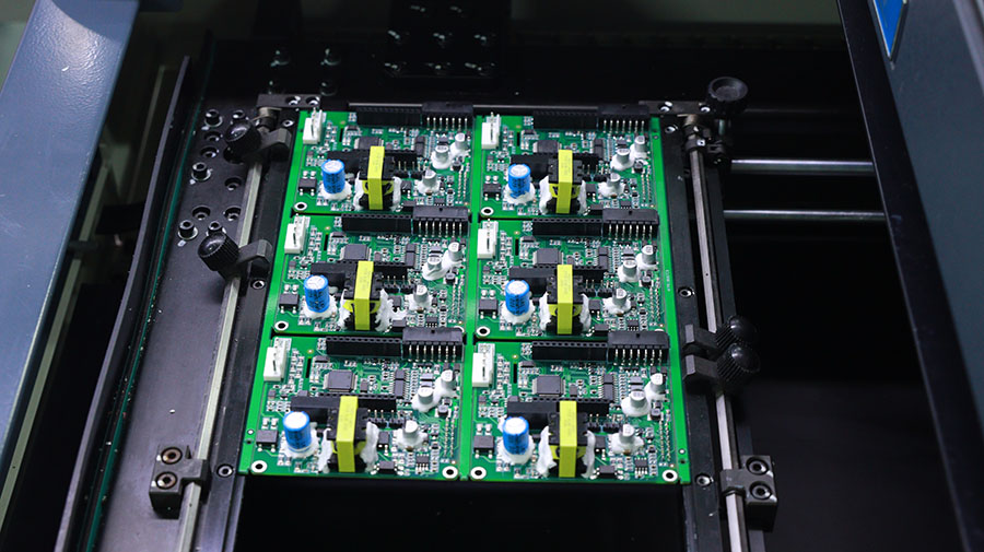
When a PCB warps by 0.5 mm or more, the uniformity of solder paste printing during the SMT placement process decreases by 23%. During the reflow soldering stage, warped boards cause the rate of cold solder joints in QFP-packaged components to rise to 2.8 times the normal level, whilst the porosity rate of BGA solder joints increases by over 40%.
1.2,How Mechanical Stress Damages Components
During the DIP insertion process on warped PCBs, the shear stress on through-hole component pins reaches 3 to 5 times the normal level. Continuous stress causes micro-cracks in the inner layer copper foil of multilayer boards, with the rate of abnormal circuit impedance reaching up to 12% after high-temperature ageing tests.
1.3,How do errors in automated testing arise?
During ICT and FCT testing, the rate of poor contact between warped boards and test fixtures increases by approximately 35%. Such contact failures account for 28% of all testing anomalies, severely impacting production efficiency.
1.4,How do assembly structural mismatches occur?
For precision-assembled products such as medical devices and industrial controllers, when PCB warpage exceeds 0.75 mm, the pass rate for housing assembly drops to less than 60%. A case study involving a medical device demonstrated that, following the resolution of shielding cover installation issues caused by warping, the product’s first-pass yield rate increased from 73% to 98.6%.
1.5,How do long-term reliability risks accumulate?
Verified through 2,000 hours of high-temperature and high-humidity testing, the fatigue life of solder joints on warped PCBA products is reduced by approximately 30% to 40%. During vibration testing, the risk of component detachment on warped boards is 2.3 times higher than on standard boards.
2.What Are the Causes of PCB Warping?
Inappropriate material selection is the primary factor; when the glass transition temperature of an FR-4 substrate is below 130°C, the risk of warping during reflow soldering increases by 45%. Defects in the laminate design can lead to a difference in the Z-axis coefficient of expansion exceeding 15% in asymmetrical laminate structures. Regarding thermal shock, a temperature difference exceeding 80°C across the board surface during wave soldering causes localised stress concentration. Regarding process parameter deviations, when the temperature rise rate during SMT reflow soldering exceeds 3°C per second, the probability of warping increases by 30%.
3. How to systematically address PCB warping
3.1,Prevention during the design phase
Provide laminate structure simulation services to predict warping trends using specialised software. Develop intelligent panelisation schemes, utilising stamp holes in conjunction with stiffener designs to reduce V-cut stress. Implement a design for manufacturability (DFM) review system to optimise thermal balance in component layout.
3.2,Production Process Control
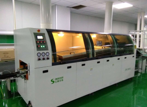
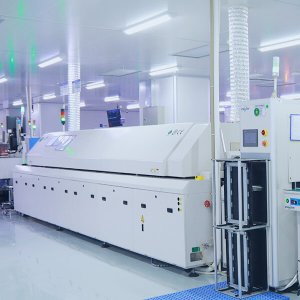
Configure fully automated PCB baking lines to precisely control pre-baking parameters at 125°C ±5°C for 4 to 6 hours. Employ three-stage reflow profile optimisation technology to maintain peak temperature deviation within ±2°C. Innovatively apply vacuum tray reflow processes to reduce warpage in large-format boards (400 mm and above) by 70%.
3.3,How to Establish Quality Assurance
Deploy 3D laser warpage detectors on the production line to monitor deformation at the 0.05 mm level in real time. Establish a database of incoming PCB warpage and implement batch-based classification management. Develop an intelligent compensation system to dynamically adjust assembly parameters for boards with minor deformation.
4.Conclusion
PCB warpage is a hidden threat to SMT assembly quality, accounting for 90% of assembly issues. Through a systematic approach combining design prevention, process control and quality assurance, warpage risks can be effectively mitigated, thereby improving PCBA manufacturing yield and long-term product reliability.