
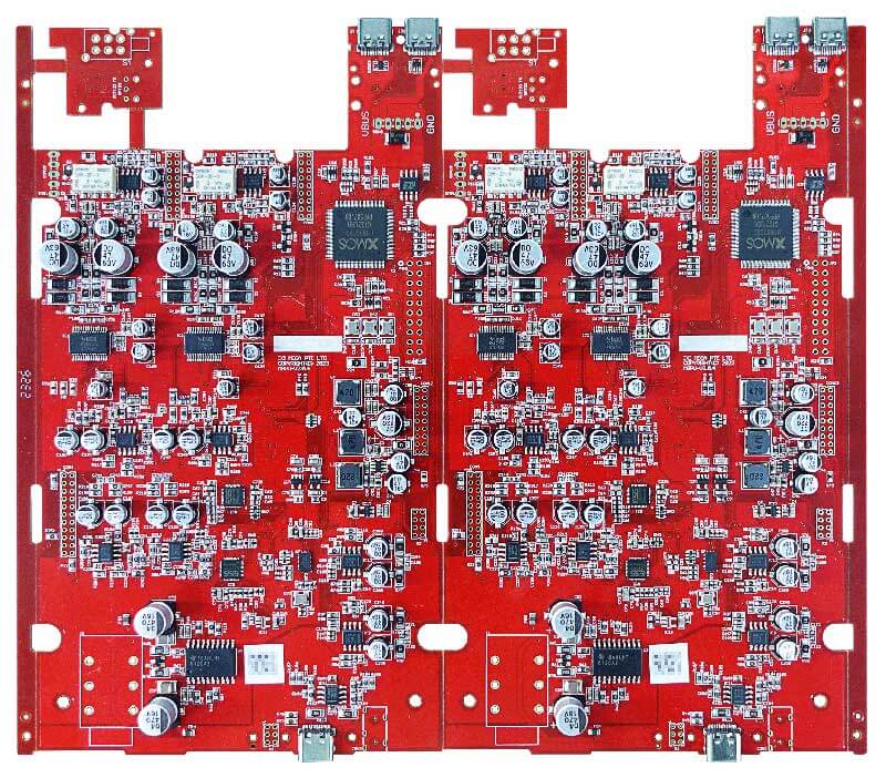
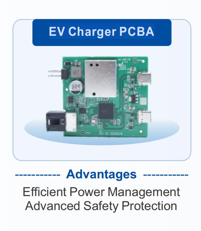
PCBA reverse engineering and prototyping involves analysing a circuit board through reverse engineering to obtain the schematic diagram and PCB design, after which a prototype is manufactured. This article outlines the core process of reverse engineering and prototyping, and analyses its technical advantages from six aspects: verifying design solutions, improving production efficiency, reducing costs, meeting personalised requirements, driving technological innovation, and ensuring product quality.
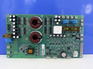
1.Definition of PCBA reverse engineering and prototyping
PCBA reverse engineering and prototyping involves analysing a circuit board through reverse engineering to obtain its schematic diagram and PCB design, and then manufacturing a prototype circuit board in accordance with the design requirements. The process of reverse engineering is not merely a simple replication; it requires scientific reconstruction based on a thorough understanding of the product’s functionality and the intent behind the circuit design. This enables clients to rapidly obtain prototypes for functional testing and product validation, thereby reducing R&D lead times and production costs.
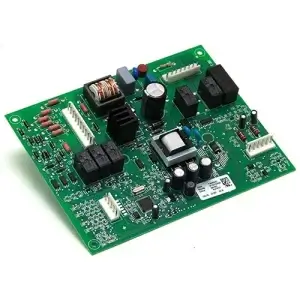
2.Core Process of PCBA Reverse Engineering and Prototyping
Requirement Confirmation: First, requirements are confirmed with the client to understand the product’s application scenarios and performance requirements, ensuring that the accuracy of the decryption and reverse engineering meets expectations.
Prototype Data Analysis: Comprehensive data is collected from the original circuit board, including layout, circuitry and BOM (Bill of Materials) information. Specialised equipment is utilised to ensure the accuracy and completeness of the collected data.
PCB Reverse Design: The schematic diagram and PCB layout are reconstructed based on the collected data, ensuring that the reverse-engineered design matches the original board.
Chip Decryption: Necessary chip decryption is carried out for boards containing encrypted chips, whilst adhering to industry regulations and the client’s compliance requirements throughout the process.
PCB Manufacturing and Component Procurement: PCBs are manufactured in accordance with the reconstructed design, and we procure components that meet the specifications on the client’s behalf, guaranteeing the quality of the boards and the traceability of the components.
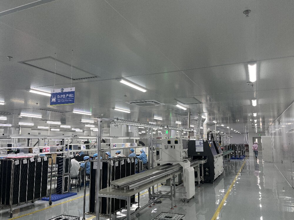
SMT/DIP Soldering: Rigorously controlled SMT/DIP soldering processes ensure the soldering quality and electrical performance of the prototype.
Assembly and Testing: The final prototype undergoes assembly and functional testing to ensure it meets the client’s expected functional and quality standards.
Delivery and Technical Support: Following delivery of the prototype, we provide further technical support and optimisation recommendations to assist the client with product validation and preparation for mass production.
3. Verifying the Feasibility and Accuracy of the Design
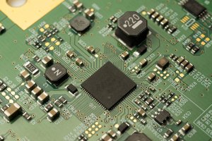
Through reverse engineering and prototyping, physical prototypes can be produced to verify the feasibility and performance of the circuit design. This helps to identify and rectify potential design issues in a timely manner, thereby preventing quality problems from arising during mass production. Should any design issues be discovered during the prototyping process, they can be promptly corrected and optimised to enhance the product’s performance and reliability.
4.Improving Production Efficiency
PCBA reverse engineering and prototyping effectively amounts to producing a finished product in advance and identifying and rectifying any shortcomings. This helps to uncover potential issues prior to formal production, thereby reducing errors and waste during the manufacturing process. Design solutions validated through prototyping can be directly applied to mass production without the need for extensive debugging or modifications, thereby shortening the production cycle.
5.Reducing Costs
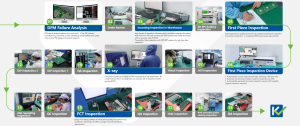
PCBA reverse engineering and prototyping can prevent material and labour wastage caused by design errors. By identifying and resolving issues in advance, rework and scrap rates during production can be reduced. The prototyping process helps to assess material requirements more accurately, optimise material management, and lower inventory costs.
6.Meeting Customised Requirements
PCBA reverse engineering and prototyping enable small-batch production tailored to customer requirements, swiftly meeting their specific needs. This flexibility allows businesses to adapt more effectively to market changes and enhance customer satisfaction.
7. Driving Technological Innovation
Through PCBA reverse engineering and prototyping, businesses can explore new manufacturing processes, materials and design methodologies. This helps improve product performance and reduce production costs, thereby driving technological innovation.
8. Ensuring Product Quality
During the PCBA reverse engineering and prototyping process, every circuit board undergoes rigorous quality inspection and control. This includes checking the circuitry to ensure there are no short circuits or open circuits, and testing components to guarantee their performance and reliability. Products validated through prototyping offer greater reliability and meet customers’ high standards for product quality.
Conclusion
PCBA reverse engineering and prototyping are vital technical tools for accelerating the research and development of electronic products and facilitating product iteration. Through a scientific reverse engineering process and rigorous quality control, it is not only possible to rapidly reproduce and validate design solutions, but also to create value for customers across multiple dimensions, including efficiency, cost, flexibility, innovation and quality. In a highly competitive market environment, mastering the core technologies of PCB reverse engineering and decryption is an effective way for enterprises to shorten R&D cycles, reduce trial-and-error costs, and seize market opportunities.
