01 / Rigid
A stable platform for electronics.
Single-sided, double-sided and multilayer designs. Align laminate, copper and tolerances with the application.

PCB manufacturing / From files to finished boards
Turn your Gerber files, material requirements and stack-up into a clear manufacturing plan—with engineering questions resolved before production.
Start with your product
Select what you know. Leave the rest to the engineering review. This is a requirements brief—not an instant price calculator.
Material, copper, dielectric thickness and via structure work together. The final stack-up is confirmed against your files.
Illustrative layers only; not a production stack-up.Your choices are added to the enquiry below. Nothing is sent until you submit the form.
Choose the board architecture
Start with mechanical, thermal and electrical requirements. We review the manufacturing route against the actual design.
Single-sided, double-sided and multilayer designs. Align laminate, copper and tolerances with the application.
Define bend areas, thickness, stiffeners and installation conditions before the fabrication route is agreed.
Coordinate stack-up transitions, mechanical drawings and assembly requirements from the start.
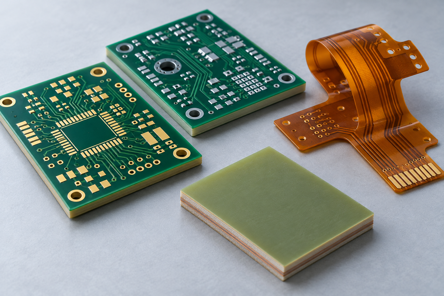
From laminate to surface finish
Material + surface finish
FR-series epoxy glass, CEM composite, high-temperature and high-frequency laminates, metal bases, ceramic and polyimide families are listed in our existing manufacturing range. Suitability and availability need project review.
Share fine-pitch features, assembly requirements and storage conditions so the finish can be evaluated with the design.
Check the fit early
Planning references from our existing service information. Final limits, material combinations and acceptance criteria are confirmed by engineering—not assumed from a headline number.
A controlled route to delivery
Engineering, manufacturing and release decisions stay connected. The exact process depends on the board structure and agreed requirements.
Review files, stack-up, materials, panelization, tolerances and manufacturing assumptions.
Output: agreed manufacturing scopeConfirm laminate, copper, drilling, imaging and plating needs against the released design.
Output: approved fabrication inputsConnect patterning, lamination, drilling, plating, solder mask, finish and profiling as applicable.
Output: boards ready for inspectionConfirm agreed inspection, electrical test, documentation, packaging and delivery requirements.
Output: reviewed shipment releaseNeed assembled boards too?
Add the BOM, placement data and test specification to your RFQ.
Before you request a quote
Have a special requirement? Email sales@keepbestpcba.com or include it with your files.
A single-layer board has one conductive layer. Multilayer boards combine multiple conductive layers separated by insulating material. The structure is chosen around routing, signal, power and mechanical requirements.
Multilayer manufacturing is included in the service. Send your required layer count and stack-up so engineering can confirm feasibility. We confirm the project-specific limit rather than applying one maximum to every material and via structure.
Timing depends on the released files, material availability, stack-up, via structure, finish, quantity and inspection requirements. Tell us your required delivery date; the quotation should state the confirmed schedule assumptions.
Send Gerber and drill files, a fabrication drawing, stack-up and board quantity. Include material, finish, copper, impedance and acceptance requirements. Native PCB/CAM files can be discussed during review. Add a BOM and assembly files if assembly is also required.
See the required-files guide →Yes—include the application and the requirements behind your specification. Laminate, finish, panelization and cost consultation can be included in the engineering conversation. Changes and alternatives should be agreed before production.
Engineering reading
Read the existing guides on manufacturing, design data and assembly.
AI-generated process illustrations · not factory photographs
PCB files ready?
Send your design files and key requirements for an engineering review and quotation.
Need assembled boards? Include your BOM too.
Prefer email?
sales@keepbestpcba.com ↗
Fields marked * are required. Phone is optional.
By submitting, you agree to our Privacy Policy.