
Heat is the silent enemy of electronics. Every active component converts some portion of its power into waste heat, and unless that heat escapes, junction temperatures climb, electrical parameters drift, and operational lifetime falls. Thermal management in PCB assembly is the set of design and process choices that keep temperatures in check and reliability high, and it is as much an electrical discipline as a mechanical one.
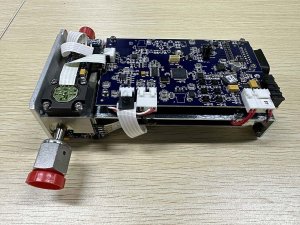
Good thermal design is not an add-on applied after the schematic is frozen. It influences trace width, layer stack-up, component placement, heatsink attachment, and even the choice of surface finish. Addressing it early prevents the expensive re-spins and field failures that follow an overheated prototype discovered too late to meet a launch date.
Conduction Paths Through the Board
Heat moves from the component through its solder joint and pad into the board, then outward by conduction. Copper is the primary highway, so adding copper area around hot parts is the simplest and most effective cooling tactic available to a board designer, and it costs little when planned into the layout rather than patched in afterward.
Solid copper pours beneath power devices spread heat across a wider region, lowering peak temperature. Connecting those pours to internal ground or power planes through vias creates a three-dimensional path into the board’s thermal mass, turning the entire stack-up into a heat spreader rather than a thin hotspot that cooks the component above it.
Thermal Vias
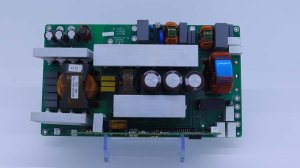
Thermal vias are plated holes placed directly under hot pads to ferry heat to inner or opposite layers. An array of small vias outperforms a single large one because more barrel surface contacts the copper and because small vias disturb the pad less. A skilled PCB assembly manufacturer recommends via count, size, and fill based on the power dissipation involved, and may specify resin-filled or capped vias for the most demanding parts to avoid voids that block heat.
Thermal Interface Materials
When a board mounts against a heatsink or enclosure, the microscopic gap between surfaces traps insulating air. Thermal interface materials such as pads, greases, phase-change compounds, or bonded films bridge that gap and dramatically improve transfer from board to metal, often reducing the dominant resistance in the entire path.
Selection depends on pressure, rework needs, and operating temperature. Too little pressure leaves air pockets; too much can stress components or squeeze material into unwanted areas. Matching the material to the mechanical design is as important as the board layout itself, and the interface is frequently the largest single resistance in the chain.
Component Placement Strategy
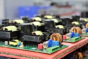
Where parts sit matters as much as how they connect. Cluster heat-generating devices away from temperature-sensitive ones such as oscillators, precision references, and sensors. Place high-power parts near board edges or mounting points where heatsinks are easier to attach and airflow is less obstructed by taller components.
Avoid trapping hot air. In enclosed products, orient boards so convection paths are unobstructed and consider venting or forced airflow where natural convection is insufficient. Even a perfectly laid-out board will overheat if the enclosure defeats the airflow it depends on, turning good engineering into a field failure.
Natural vs Forced Convection
Natural convection relies on rising warm air and works for low-power designs with adequate surface area and ventilation. Forced convection, via a fan or blower, multiplies heat removal and is often necessary for dense power electronics. The choice shapes the entire enclosure and should be settled during architecture, not after the board is built and found to run hot.

When forced air is used, direct it across the hottest components first and avoid dead zones behind tall parts. Computational or even simple hand calculations of airflow and pressure drop prevent the common mistake of specifying a fan that cannot deliver air where it is needed most.
Thermal Relief and Soldering
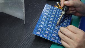
Large copper areas pull heat away during soldering, making joints hard to form and prone to cold joints. Thermal relief spokes connect pads to planes with thin links that limit heat sinking while preserving most of the thermal path in operation. This balance keeps both assembly and cooling performant without sacrificing either goal.
A detail-oriented one-stop PCBA solution tunes thermal relief for each pad so reflow stays reliable without sacrificing too much conduction. The same pad that needs relief for soldering may need a direct connection for operation, and the compromise must be engineered rather than guessed from a generic rule.
Simulation Before Fabrication
Thermal simulation tools estimate junction temperatures and hotspot distribution before a single board is built. Running these early catches problems that would otherwise surface only after expensive prototyping and field returns, and they let engineers compare cooling strategies virtually at negligible cost compared with hardware spins.
Modern tools couple electrical power maps with board geometry and enclosure airflow, producing realistic predictions rather than rules of thumb. Designs validated this way enter production with confidence instead of hope, and changes that would cost weeks in hardware are resolved in hours of compute time.
Practical Cooling Checklist
A useful discipline is to walk each major heat source through the full path: die, package, solder, pad, via array, plane, interface material, heatsink, and ambient. The weakest link in that chain defines the board’s thermal ceiling, and strengthening anywhere else yields nothing until that link improves, so diagnosis should precede action.
Thermal discipline pays compounding dividends: higher reliability, smaller heatsinks, quieter fans, and the confidence to push performance closer to the component’s true limits. It is among the highest-return investments a hardware team can make, and it is far cheaper than explaining a field failure to a customer.
