

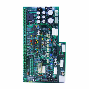
The PCBA process margin refers to the edge area of a PCB, encompassing elements such as edge dimensions, via design, board edge finishing methods and mechanically reinforced areas. This article analyses the key value of process margin design in five areas: improving production efficiency, ensuring product stability, enhancing assembly compatibility, facilitating testing and debugging, and improving product appearance.

1.Core Concepts of the Process Margin
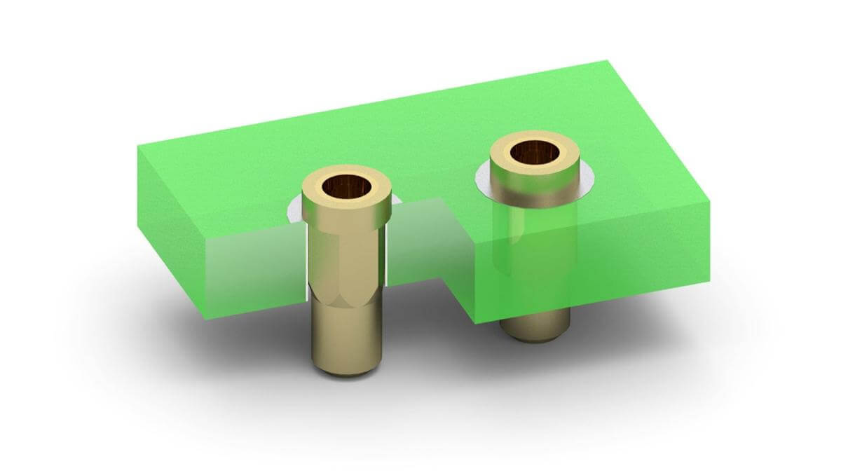
The process margin in PCBA design typically refers to the edge region of a PCB; the design of this section must take into account multiple factors, including stability during manufacturing, assembly, transport and use. During the PCBA design process, the design of the process margin encompasses edge dimensions, via design, board edge finishing methods and mechanically reinforced areas.
Edge dimensions determine the length and width of the PCB, as well as the distance from external connection points. Via design involves the placement of vias at the board edges; these vias are not only used for electrical connections but may also affect subsequent assembly processes. Board edge processing methods include V-cut, slot cutting and laser cutting; different cutting methods have varying effects on the performance and stability of the board edges. Mechanical reinforcement areas are typically incorporated at the board edges to ensure the stability of the PCB during subsequent handling, thereby preventing excessive bending and damage.
A well-designed process margin ensures a smoother PCB production process and prevents potential processing or assembly issues arising from poor design.
2.Improving Production Efficiency and Reducing Costs
Designing an appropriate process margin can significantly improve production efficiency and reduce overall production costs. A suitable V-cut design reduces the difficulty of cutting PCBs during production and prevents waste caused by board breakage or irregular cuts. By optimising the design of the process margins, equipment wear during PCB cutting can be reduced, production cycles shortened, and consequently production costs lowered.
3. Ensuring Product Stability and Reliability
The design of the board edges is crucial to the mechanical performance and stability of the PCB. Particularly during production, the strength and stability of the PCB edges directly affect the accurate placement of components and the smooth progression of subsequent soldering processes. When designing process margins, the inclusion of appropriate edge reinforcement zones can effectively prevent warping or breakage of the PCB during transport, assembly and use, thereby ensuring the reliability of the final product.
4.Enhancing Compatibility for Assembly and Connection
In many cases, PCBA designs require connection to other components or systems. The design of the board edges must take the compatibility of these connections into account. Process margins can provide suitable interfaces and space for external connectors, plugs or terminals. An appropriate design ensures more precise installation of these components, whilst reducing the risk of poor connections or poor contact.

5.Improving Convenience for Testing and Debugging
Testing and debugging are inevitable stages in the PCBA production process. A well-designed process margin helps production staff secure the circuit board more effectively during testing, thereby reducing potential errors. Furthermore, a well-designed edge area can provide additional interfaces and test points during the testing phase, facilitating inspection and maintenance by debugging personnel.
6.Enhancing Product Aesthetics and Brand Image
For many consumer electronics products, PCBs must not only meet functional requirements but also align with the product’s aesthetic design. A well-designed process margin can make the PCB’s appearance more aesthetically pleasing and tidy, further enhancing the product’s visual appeal and sense of quality. This also plays a significant role in establishing the brand image.
Conclusion
PCBA process margin design serves as the bridge between circuit functionality and manufacturing implementation. Scientific planning of edge dimensions, the selection of appropriate processing methods, and thorough mechanical reinforcement design not only improve production efficiency and reduce costs but also ensure product stability, assembly compatibility, testing convenience and aesthetic quality. Incorporating process margin design into the DFM (Design for Manufacturability) framework is a fundamental step in achieving high-quality PCBA delivery.