

PCBs are categorised into three main types based on their structure: single-layer boards, multi-layer boards and special material boards, each suited to different electronic applications. This article analyses the manufacturing processes, characteristics, applications and considerations for five types of PCBs—single-layer, multi-layer, flexible, aluminium-based and ceramic boards—providing a comprehensive reference for PCB selection and manufacturing.
1.Characteristics and Applications of Single-Layer PCBs
Single-layer PCBs feature a simple structure comprising a single conductive layer, making them suitable for use in small electronic devices, household appliances and simple control circuits. Their core advantages lie in low manufacturing costs, straightforward processes and ease of automation.
2.Manufacturing Process for Single-Layer PCBs
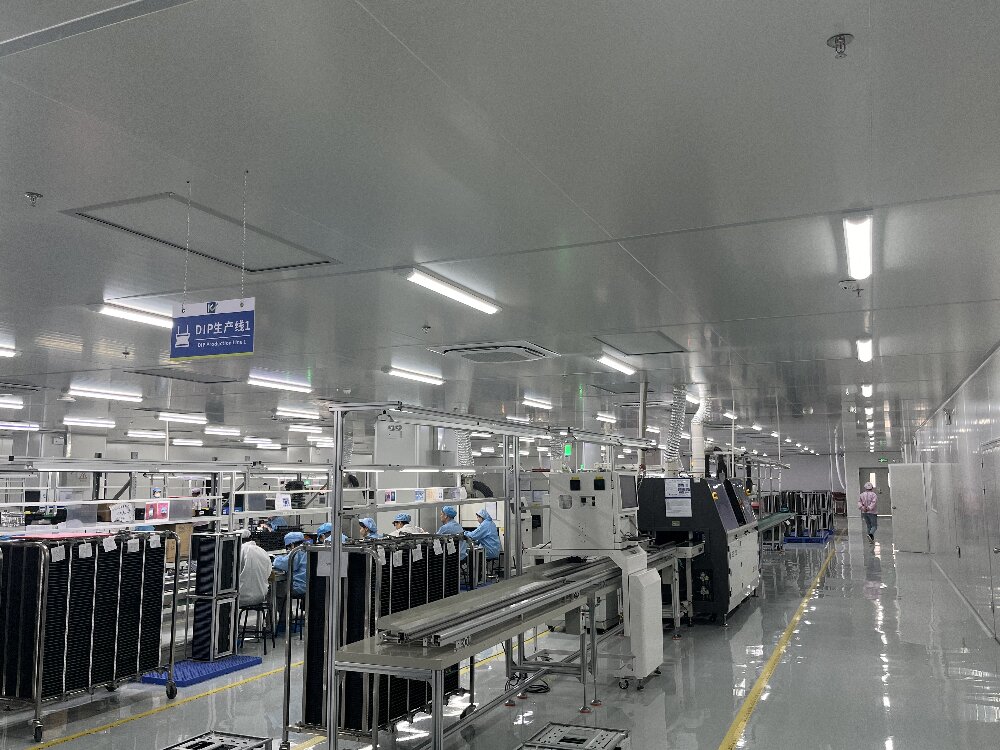
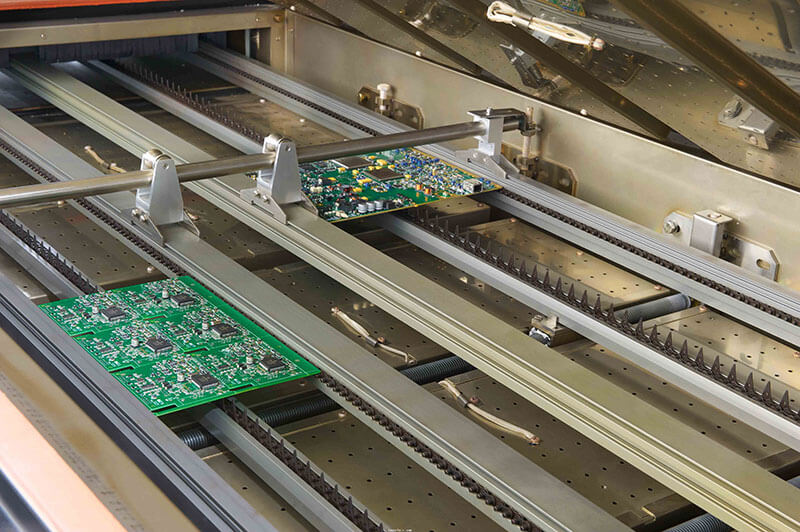
During the PCB design phase, a single-layer board file containing component layout and routing is created according to product requirements, ensuring that traces are kept as simple as possible and minimising crossovers. During the component procurement stage, the required electronic components—such as resistors, capacitors and chips—are sourced. As single-layer boards require fewer types of components, procurement costs are low. In the surface-mount and through-hole assembly stages, components are mounted onto the PCB using SMT (Surface Mount Technology) or DIP (Dual In-Line Package) processes. For the soldering process, single-layer boards typically employ reflow soldering or wave soldering, which are straightforward processes that facilitate automated production. Following soldering, functional testing is carried out during the testing and inspection stage to ensure the integrity and stability of the circuit.
3.Considerations for Single-Layer PCB Manufacturing
When routing traces, avoid excessively long leads to minimise electromagnetic interference. When mounting components, pay attention to polarity and orientation to prevent incorrect installation, which could lead to functional failure.
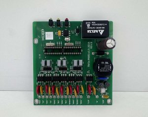
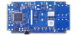
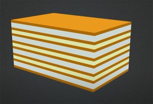
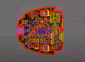
4.Characteristics and Applications of Multilayer PCBs
Multilayer PCBs consist of multiple conductive layers stacked together and are suitable for high-density, high-performance electronic products, such as computer motherboards, communication equipment and industrial controllers. Inter-layer signal integrity and electromagnetic compatibility are key design challenges.
5.Multilayer PCB Manufacturing Process
The PCB design phase requires complex design tools and methodologies, with a focus on inter-layer signal integrity and electromagnetic compatibility. The component procurement stage typically requires high-precision, high-performance components, with particular attention to be paid to specification compatibility during procurement. The surface-mount and through-hole assembly stages demand higher process precision, usually employing high-precision SMT (Surface Mount Technology) processes. The soldering process may include reflow soldering and selective wave soldering to ensure the reliability of solder joints. The multi-layer inspection stage requires automated optical inspection (AOI), in-circuit testing (ICT) and functional testing to ensure signal integrity on every layer.
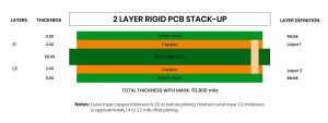
6.Considerations for Multi-Layer PCB Manufacturing
The design must clearly define signal, ground and power planes to minimise signal crosstalk. During production, the alignment accuracy of each layer must be strictly controlled to prevent electrical performance degradation caused by misalignment between layers.
7.Characteristics and Applications of Special Material PCBs
Special material PCBs, such as flexible printed circuits (FPCs), aluminium-clad laminates and ceramic boards, are typically used in specific environments or scenarios with high-performance requirements, such as LED lighting, automotive electronics and medical devices. The material properties dictate specific requirements for design and manufacturing.
8. Process Flow for Special Material PCB Manufacturing
During the PCB design phase, the design must account for material properties; for instance, the bending radius must be considered for flexible boards, whilst heat dissipation pathways must be optimised for aluminium-based boards. During component procurement, high-temperature-resistant, high-thermal-conductivity or flexible components must be selected according to the requirements of the special materials. During the surface-mount and through-hole assembly phases, flexible boards require special support fixtures to assist with placement, whilst aluminium-based boards require high-temperature-resistant adhesive. During the soldering process, special materials may require dedicated techniques, such as spot soldering or selective soldering. In the functional testing phase, environmental tests—including high-temperature, high-humidity and vibration testing—are added to account for the specific properties of different materials.
9.Precautions for Special Material PCB Manufacturing
When processing flexible boards, excessive bending must be avoided to prevent compromising electrical conductivity and service life. During the soldering of aluminium-based boards, careful temperature control is essential to prevent overheating that could damage components and the insulation layer.
Conclusion
Single-layer, multi-layer and special material PCBs each have their own applicable scenarios and process characteristics. Single-layer PCBs prioritise simplicity and efficiency, multi-layer PCBs emphasise precise layering, whilst special material PCBs require adaptation to the specific properties of the materials. Understanding the manufacturing processes and precautions for each type of PCB is a fundamental capability for ensuring product performance, reliability and cost-effectiveness.