The PCBA Manufacturing Process: A Step-by-Step Guide
A PCB design file is not a product. It is a blueprint. Transforming that blueprint into reliable, electrically functional assemblies requires a manufacturing process that balances speed, precision, and repeatability. we have refined this process across millions of assembled boards. This guide walks through each stage exactly as it happens on our production floor.
Stage 1: Pre-Production Engineering and DFM Review
Before a single component is placed, the engineering team validates that the design can actually be built at volume. This step prevents expensive surprises during production.
Bill of Materials Validation — Every part number is cross-referenced against current distributor inventory. Obsolete components are flagged. Long-lead-time items are identified and procurement is initiated.
Gerber and Centroid File Review — Engineers verify component orientations, polarity markings, and footprint alignments match the physical reels that will feed the machines.
Design for Manufacturability Feedback — Keepbest returns DFM feedback within 48 hours. Common flags include insufficient component spacing, missing fiducials, tombstone-prone pad geometries, inadequate test point coverage, and high aspect ratio vias.
Stencil Design — A laser-cut stainless steel stencil (100–150 microns thick) is fabricated with aperture geometries calculated for each pad. Stencil fabrication takes 1–2 days and is included in standard NRE.
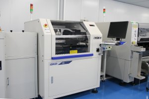
Stage 2: Solder Paste Printing
The bare PCB is loaded into a printer. A squeegee forces solder paste through the stencil apertures onto every pad that will receive a surface-mount component.
Paste Composition — Modern lead-free assemblies use SAC305 solder paste suspended in a flux vehicle. Paste is stored at 0–10°C and equilibrated to room temperature for 4 hours before opening.
3D Solder Paste Inspection (SPI) — Immediately after printing, the board enters an SPI system that uses laser triangulation to measure paste volume, height, and alignment on every pad. Catching paste defects here prevents approximately 70% of downstream soldering issues.
Stage 3: Component Placement
The pasted board enters a high-speed pick-and-place machine. Vacuum nozzles retrieve components from tape-and-reel feeders, verify identity and orientation with vision systems, and place them onto the paste deposits.
Machine Capability — we operates Panasonic NPM placement lines capable of placement accuracy of ±35 microns at 3 sigma, component range from 0201 passives to 50 mm QFPs, finest pitch of 0.3 mm QFP and 0.4 mm BGA, and speeds exceeding 100,000 placements per hour.
Post-Placement AOI — After all components are placed, an AOI system captures images of every component to detect missing parts, reversed polarity, skewed placement, and wrong components.

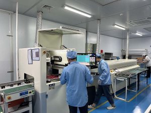
Stage 4: Reflow Soldering
The populated board travels through a multi-zone conveyorized reflow oven. The temperature profile follows a precise thermal curve.
The Reflow Profile — Preheat (90–150°C) gradually evaporates solvents. Soak (150–180°C) equalizes temperature. Reflow peak (235–250°C for SAC305) forms metallurgical bonds. Cooling solidifies solder into fine grain structure.
Nitrogen Atmosphere — For medical, automotive, and high-reliability assemblies, we uses nitrogen reflow to reduce oxide formation and improve wetting quality.
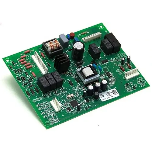
Stage 5: Through-Hole Insertion and Soldering
Not all components are suited to surface-mount assembly. Power connectors, large electrolytic capacitors, and transformers typically use through-hole leads.
Wave Soldering — For pure through-hole boards in high volume.
Selective Soldering — For mixed-technology boards with SMT already populated on the underside. This avoids exposing previously soldered SMT components to a second thermal cycle.

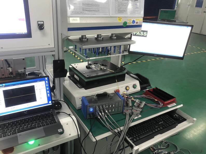
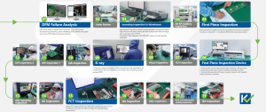
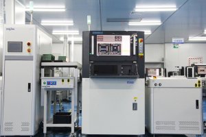
Stage 6: Inspection and Testing
No functional board ships from our without passing rigorous inspection gates.
SPI — 3D laser scanning verifies paste volume before placement begins.
AOI (post-placement) — Catches missing components and wrong polarity.
AOI (post-reflow) — Detects solder bridges, insufficient solder, tombstoning.
X-ray (AXI) — Penetrates BGAs and QFNs to reveal voids and bridging.
ICT — Bed-of-nails or flying-probe fixtures verify electrical integrity.
FCT — The board is powered in a simulated operating environment.
Stage 7: Final Cleaning, Packaging, and Logistics
Before shipment, boards receive final treatment and protective packaging. Boards are placed in anti-static trays, vacuum-sealed with desiccant, and labeled with lot numbers and serial numbers. Each shipment includes a certificate of conformance and component traceability records.
Frequently Asked Questions
Q: What is the difference between SMT and THT assembly?
SMT places components directly onto the board surface and solders them during reflow. THT inserts leads through drilled holes and solders them from the underside. SMT enables smaller, denser assemblies. THT provides stronger mechanical bonds.
Q: Why does my prototype cost more per board than mass production?
Prototype runs carry the full burden of NRE costs across a small number of units. At 10,000 units, that overhead is amortized to pennies per board.
Q: What causes the most common production delays?
Component availability is the leading cause. A single long-lead-time FPGA can hold up an entire lot. we identifies long-lead items during BOM review.
Q: How do I know if my design needs X-ray inspection?
If your board contains BGA, QFN, DFN, or other hidden-joint packages, X-ray inspection is essential. we automatically includes 100% X-ray on all such assemblies.
Q: What files do I need to provide for a production quote?
Gerber RS-274X files, complete BOM with manufacturer part numbers, and centroid file with X-Y coordinates and rotation data.
Q: Can we handle both prototyping and mass production?
Yes. We apply the same process discipline to 5-unit prototype runs and 50,000-unit production. No scaling surprises.
Ready to move your design into production? Send your Gerbers, BOM, and centroid files to the Keepbest engineering team. We will return DFM feedback within 48 hours.