


In SMT production, packaging types such as QFP, BGA, QFN and CSP present distinct process challenges due to their structural differences. This article analyses the causes of defects—including placement misalignment, cold solder joints and voids—in these four common packaging types, and provides systematic optimisation solutions covering four key areas: solder paste printing, placement accuracy, reflow temperature and PCB design.

1.Overview of Package Types and Process Challenges
QFP, BGA, QFN and CSP are the mainstream package types in SMT production. Due to differences in structure, dimensions and thermal design across these package types, the requirements for controlling process parameters also vary.
2.Common Issues with QFP Packages and Their Causes
Significant placement misalignment and errors, as well as cold solder joints or bridging, are the primary manifestations of these issues.
Uneven solder paste printing is the primary cause. As QFP pins are arranged along the edge of the board, insufficient or uneven solder paste application can prevent adequate wetting of the pins during soldering, leading to cold solder joints or solder bridges.
Inadequate placement accuracy is the second cause. High-density pin arrangements require the placement machine to possess extremely high positioning accuracy; even the slightest misalignment can cause cross-soldering issues.
Inappropriate reflow temperature profiles are the third cause. Insufficient temperature or excessively rapid heating can both affect the melting and flow of the solder paste, resulting in suboptimal connections at the solder joints.

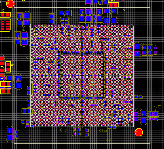
3. Common Issues and Causes in BGA Packaging
The primary manifestations of these issues include voids or cold solder joints within the solder balls, as well as hidden defects in the solder joints that are difficult to detect.
Inadequate control of solder paste printing and reflow parameters is the primary cause. BGA packages utilise spherical solder balls, and their soldering quality relies heavily on the correct deposition and uniform distribution of the solder paste. Improper printing processes or insufficient reflow temperatures can easily lead to the formation of pores and voids within the solder balls.
PCB flatness issues are the second cause. BGA packages demand high substrate flatness; if the PCB warps in certain areas, it will result in uneven component placement, thereby affecting the formation of solder joints.
Ball position deviation and component positioning errors are the third cause. As BGA solder balls are concealed beneath the package, even minor deviations during placement may prevent proper contact after soldering, resulting in cold solder joints or poor solder joints.

4.Common Issues and Causes in QFN Packaging
Poor soldering of the central large pad, voids and uneven solder joints are the most prominent manifestations of the problem.
Inappropriate control of solder paste deposition is the primary cause. QFN packages typically feature large heat-dissipating pads; if the amount of solder paste printed is either excessive or insufficient, this may lead to uneven solder distribution during the reflow process, resulting in voids or poor solder joint integrity.
Inadequate venting is the second cause. As the pads on the bottom of the package are large, if the volatile gases generated during heating are not vented properly, bubbles are likely to form beneath the pads, affecting the strength of the solder joints.
Reflow soldering temperature control is the third cause. QFN packages are relatively sensitive to temperature profiles; insufficient temperature or an excessively short hold time can lead to inadequate solder wetting, resulting in cold solder joints.

5.Common Issues and Causes in CSP Packaging
The primary issues arise from the minute size of the packages, which increases placement difficulty and leads to suboptimal solder joint formation, making missed solder joints or short circuits likely.
The primary cause is the extremely high placement accuracy required due to the minute dimensions. As CSP packages are similar in size to bare chips, even the slightest placement deviation can lead to poor soldering.
The second cause is the difficulty in controlling solder paste deposition. Given the limited surface area of the package, the quantity and positioning of the solder paste are critical to joint quality; the slightest error can result in either excess or insufficient solder paste.
Equipment compatibility issues are the third cause. CSPs place high demands on the resolution of SMT equipment and the accuracy of camera recognition; if equipment calibration is inaccurate, this can similarly lead to placement deviations and solder joint defects.
6.Improvement Measures and Process Optimisation
In response to the issues commonly encountered with the aforementioned package types, the industry generally adopts the following optimisation measures.
Optimise the solder paste printing process. Ensure uniform solder paste deposition by finely adjusting stencil parameters, solder paste viscosity and printing speed.
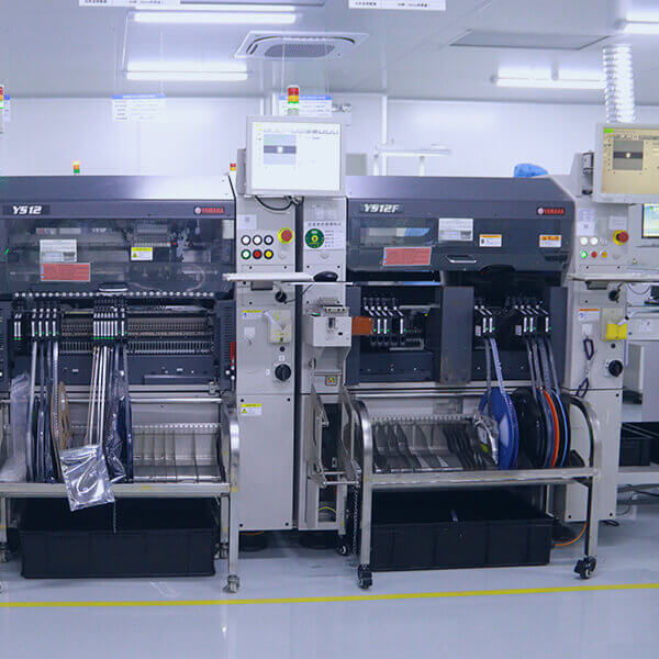
Enhance placement machine accuracy. Regularly calibrate placement equipment, optimise programs and adjust camera parameters to ensure accurate component positioning.
Strictly manage reflow soldering temperatures. Develop scientific temperature profiles and adjust the preheating, isothermal, reflow and cooling stages according to different package types to ensure sufficient solder wetting.
Improve PCB design. Maintain substrate flatness and rationally plan routing and pad dimensions to reduce process complexity.

Conclusion
The quality of SMT package soldering forms the foundation of electronic product reliability. By precisely identifying the process weaknesses of the four package types—QFP, BGA, QFN and CSP—and systematically optimising the four key stages of solder paste printing, placement accuracy, reflow temperature and PCB design, it is possible to effectively reduce defect rates such as cold solder joints, voids and bridging, thereby improving product first-pass yield and long-term reliability.