
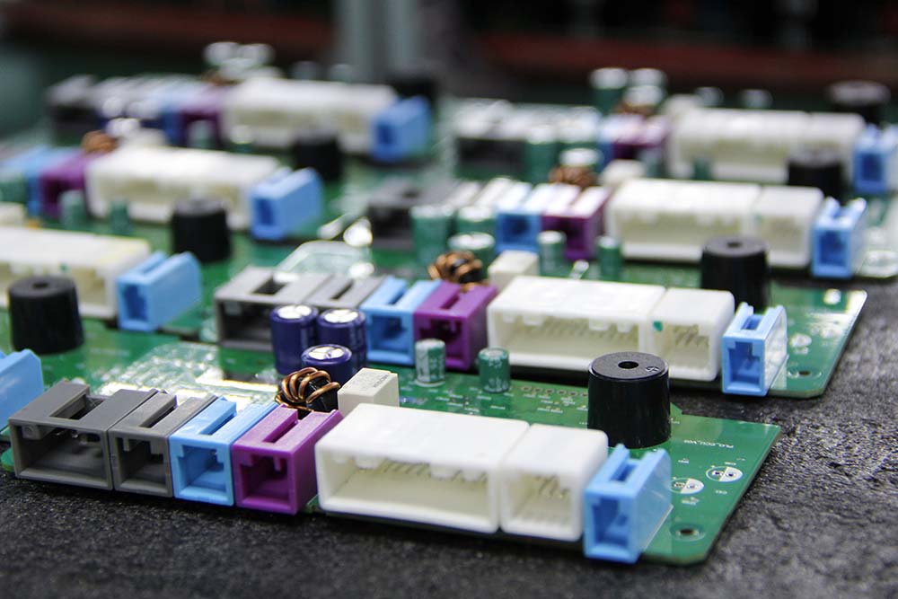
A PCBA that looks perfect can still fail in the field. Solder joints hidden beneath BGA packages, microscopic cracks in capacitors, and parametric drift in semiconductors are invisible to the human eye but catastrophic in operation. The difference between a reliable product and a warranty disaster is the depth and discipline of the testing protocol applied before shipment.

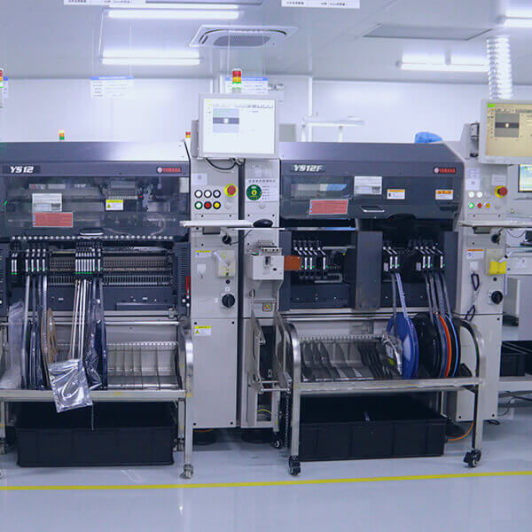
At Keepbest, quality is not a department. It is a layered architecture that begins before the first component is placed and continues until the board is sealed in its shipping package.

The Economics of Quality
Every defect caught early saves exponentially more than the same defect caught late.
Stage of Discovery | Relative Cost to Fix
Design phase (DFM catch) | 1x
Paste printing (SPI catch) | 1x
Component placement (AOI catch) | 3x
After reflow (AOI catch) | 5x
In-circuit test (ICT catch) | 10x
Functional test (FCT catch) | 20x
In customer’s hands (field failure) | 100x+
Layer 1: Solder Paste Inspection (SPI)
SPI examines solder paste deposits immediately after stencil printing and before any components are placed. It is the earliest possible quality gate.
3D laser triangulation measures paste volume, height, area, and alignment on every pad. Catching insufficient paste, excessive paste, paste misalignment, stencil aperture clogging, and slump before placement begins prevents roughly 70% of downstream soldering issues.
At ours, SPI is mandatory on every board. Any pad with paste volume outside plus or minus 25% of target triggers automatic rework before the board proceeds.
Layer 2: Automated Optical Inspection (AOI)
AOI uses high-resolution cameras and image analysis to detect visible assembly defects at two stages: after component placement and after reflow soldering.
Post-placement AOI catches missing components, wrong components, reversed polarity, skewed placement, and damaged components while they are still easy to fix.
Post-reflow AOI detects solder bridges, insufficient solder, tombstoning, component shift, solder balls, and lifted leads.
We have deployed deep-learning-enhanced AOI systems that significantly outperform traditional rule-based algorithms, detecting subtle anomalies that older systems miss entirely.
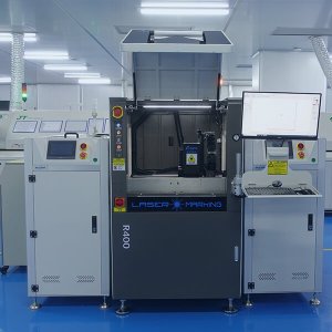
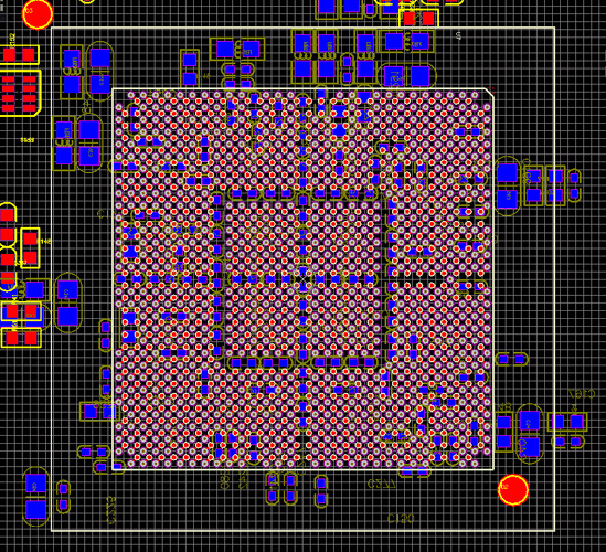
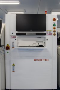
Layer 3: Automated X-Ray Inspection (AXI)
AOI cannot see what is hidden. BGAs, QFNs, LGAs, and other bottom-terminated packages obscure their solder joints from optical view. X-ray inspection penetrates these packages to reveal the hidden world beneath.
2D X-ray shows solder joint integrity, void percentage, and bridging. 3D X-ray and computed tomography create cross-sectional slices that reveal BGA voiding, head-in-pillow defects, bridging under packages, insufficient wetting, and QFN heel fillet cracks.
Keepbest performs 100% X-ray on every assembly containing hidden-joint components. No exceptions.

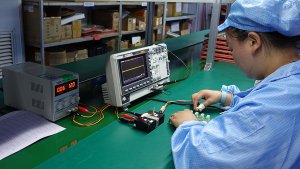
Layer 4: In-Circuit Test (ICT)
ICT verifies electrical integrity by contacting test points with spring-loaded probes. It confirms every component is the correct value, correctly oriented, and properly connected.
Flying probe ICT uses movable probes that travel to each test point sequentially. No custom fixture required. Best for prototypes and low-volume production.
Bed-of-nails ICT uses a custom fixture with hundreds of spring probes. All points contact simultaneously. Much faster per board but requires fixture NRE.
ICT verifies resistance, capacitance, inductance, diode forward voltage, transistor gain, shorts, and opens.
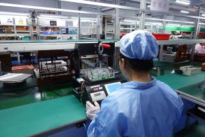
Layer 5: Functional Circuit Test (FCT)
FCT validates that the board performs its intended function in a realistic operating environment. It is the final confirmation that design, components, and assembly have converged into a working product.
A custom test fixture simulates operating conditions with power supplies, load simulation, signal generators, measurement instruments, and microcontroller interfaces.
The typical FCT protocol includes power-on self-test, communication test, analog verification, digital functional test, load and stress test, calibration, and final parameter logging.
Layer 6: Environmental and Reliability Testing
For applications where failure is not an option, environmental testing subjects boards to accelerated stress.
Test | Conditions | Purpose |
Thermal cycling | -40°C to +125°C | Reveals solder joint fatigue
High-temp operating life | Max rated temperature | Accelerates semiconductor degradation |
Temperature-humidity bias | +85°C, 85% RH | Reveals moisture ingress and corrosion |
Mechanical shock/vibration | Specified G-force | Verifies structural integrity |
ESD testing | Human body model | Verifies protection circuit effectiveness |
Choosing the Right Testing Stack
Application | Minimum Testing | Recommended | Enhanced |
Consumer electronics | Post-reflow AOI | AOI + ICT | AOI + ICT + FCT |
Industrial controls | AOI + ICT | AOI + ICT + FCT | Full stack + thermal cycling |
Medical (non-life-support) | AOI + X-ray + ICT | AOI + X-ray + ICT + FCT | Full stack + environmental |
Medical (life-support) | AOI + X-ray + ICT + FCT | Full stack | Full stack + full environmental |
Automotive (safety-critical) | Full stack | Full stack + environmental | Full stack + AEC-Q100 |
| Aerospace / defense | Full stack + environmental | Full stack + full environmental + radiation | AS9100 + mission-specific |
Frequently Asked Questions
Q: What is the difference between AOI and X-ray inspection?
AOI uses visible-light cameras for surface features. X-ray penetrates opaque packages to inspect hidden joints under BGAs and QFNs. Both are necessary for complete coverage.
Q: Do I need ICT if I already have AOI and X-ray?
Yes. AOI and X-ray verify physical assembly quality. ICT verifies electrical correctness including wrong component values, reversed diodes, and parametric drift.
Q: What is the minimum test point coverage for effective ICT?
One accessible test point per electrical net, minimum 1.0 mm diameter and 2.5 mm clearance from components.
Q: Can Keepbest provide test data with every shipment?
Yes. We provide certificates of conformance, ICT logs, FCT reports, and AOI/X-ray images upon request.
Need help defining the right testing stack? Send your design files and application requirements to our quality engineering team.