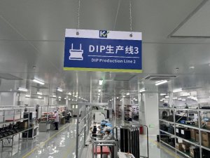
PCB Assembly Best Practices: From DFM to Final Quality Control
Electronic products succeed or fail on the manufacturing floor. A smart circuit design that cannot be assembled consistently at scale creates downstream costs far exceeding any engineering elegance it might represent. Following established PCB assembly best practices — from design review through final quality inspection — bridges the gap between concept and reliable production.
The most effective practices are applied early and reinforced continuously. What follows are the critical checkpoints that experienced teams use to ensure boards are not just buildable, but built well, with high first-pass yield and predictable long-term reliability.
Design for Manufacturability: Start with DFM
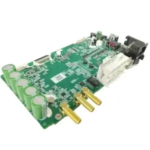
Design for manufacturability is the single highest-leverage activity in the PCB assembly workflow. The cost of fixing a design issue grows by roughly 10x at each stage: schematic entry, layout, prototyping, and production. A DFM review during layout takes an hour; re-spinning a board in production costs weeks and thousands of dollars.
Critical DFM Checks
Component-to-edge clearance should be at least 3mm for panelized boards. Components placed too close to the board edge risk damage during depaneling. This is especially critical for ceramic capacitors, which can develop micro-cracks from mechanical stress that only surface as field failures months later.
Pad size and solder mask relief must match component footprints precisely. Overly large pads increase tombstoning risk on small passives. Insufficient pad-to-mask clearance causes solder mask encroachment, reducing the solderable area and weakening joints.
Thermal relief design on pads connected to large copper planes prevents cold joints during reflow. Copper planes act as heat sinks that prevent solder from reaching proper wetting temperature. A 4-spoke thermal relief pattern, typically 0.25mm wide, provides the right balance between thermal isolation and electrical connectivity.
Fiducial marks should appear on both the panel frame and individual boards. Global fiducials enable pick-and-place machines to locate the panel; local fiducials compensate for board-level variation. Three fiducials per board arranged in an L-shape provide both X-Y alignment and rotational correction.
Polarity markings must remain visible after assembly. Silkscreen indicators hidden under component bodies provide no value. Using pin-1 indicators on both silkscreen and copper layers ensures unambiguous orientation cues that survive the assembly process.
An experienced PCB assembly manufacturer catches DFM issues that automated checkers miss — especially around process-specific nuances like wave solder pallet clearance or selective soldering access.
Component Sourcing and BOM Management
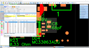
A well-managed bill of materials separates smooth builds from weeks of procurement delays.
Lifecycle validation should be performed on every BOM line item. Many manufacturers mark parts as “not recommended for new design” long before formal obsolescence. Catching NRND status during design review, not procurement, prevents costly last-minute redesigns.
Approved manufacturer lists with at least two qualified sources per critical component prevent single-supplier dependency. During recent semiconductor shortages, designs with validated alternates continued production while competitors faced months-long delays.
Moisture sensitivity level affects component handling and storage requirements. MSL 3 parts, common for QFN and BGA packages, require baking if floor-life exposure is exceeded. Including MSL ratings on the BOM ensures the assembly team knows which parts need dry-pack storage.
Accurate package geometries prevent pick-and-place nozzle issues. A 0402 resistor and 0402 capacitor can have subtly different body dimensions requiring different nozzle sizes. Machine-verified package data, not datasheet approximations, should feed into placement programming.
SMT Process Control
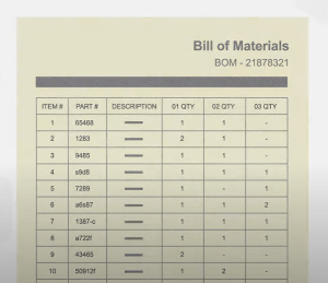
Once the design and BOM are solid, process control on the SMT line determines yield. Roughly 60% of SMT defects originate at the solder paste printing stage, making it the highest-value area for process investment.
Solder paste printing demands tight control of several variables. Stencil thickness must match the finest-pitch component: 0.1mm works for 0.5mm pitch QFPs but may deposit insufficient paste for larger power components. Step stencils with zone-specific thickness solve this trade-off.
Solder paste inspection after printing catches insufficient volume, bridging, and smearing before components are placed. Correcting a paste issue at SPI takes seconds; correcting after reflow requires a full rework cycle costing orders of magnitude more.
Environmental control — temperature at 22-26°C and humidity at 40-60% RH in the printing area — prevents paste degradation. Both drying out and moisture absorption degrade print quality and downstream yield.
Reflow profile development should be done per assembly, not just per paste specification. A board with a large BGA and tiny 0201 passives needs a profile that satisfies both thermal requirements. Thermocouple attachment to representative joints provides empirical data rather than relying solely on oven setpoints.
Nitrogen reflow improves wetting and reduces oxidation, particularly important for lead-free soldering with ENIG or OSP surface finishes. The incremental nitrogen cost is typically justified for assemblies with fine-pitch components below 0.4mm.

Mixed-Technology Assembly Control
For boards combining surface-mount and through-hole components, process sequencing is critical. The standard sequence runs SMT reflow first, then through-hole wave soldering — but this introduces thermal stress to bottom-side SMT components.
Bottom-side SMT parts need glue-dot anchoring to survive wave soldering. Sensitive components like crystals and connectors should be placed on the top side only, away from the wave.
Selective soldering has largely replaced hand soldering for mixed-technology production. A programmable nozzle applies solder only to specific through-hole joints, avoiding thermal stress on nearby SMT parts. While slower per joint than wave soldering, it eliminates pallet costs and reflow damage risk.
Press-fit connectors eliminate soldering entirely for high-reliability through-hole connections. The mechanical interference fit creates a gas-tight connection that outperforms soldered joints in vibration and thermal cycling environments. The trade-off is higher connector cost and tighter hole tolerance requirements.
Quality Inspection: Build Quality In, Don’t Inspect It In
Testing is not an afterthought — it is the feedback loop that drives continuous process improvement across an one-stop PCBA solution operation.
First-article inspection should apply to every new production run, not just new designs. Even previously built assemblies can drift due to component batch variations, stencil wear, or subtle machine calibration shifts.
3D AOI systems measure solder joint volume and shape, not just 2D appearance. This catches defects that traditional 2D AOI misses, especially for challenging joints like J-lead and chip components. AOI programming should be updated whenever a board revision changes component placement — stale programs generate false failures that slow inspection and desensitize operators.
X-ray inspection is essential for any board with BGA, QFN, or bottom-terminated components. These packages hide connections under the component body where optical methods cannot reach. 2D X-ray verifies ball shape and voiding; 3D CT X-ray adds layer-by-layer analysis for mission-critical assemblies.
Functional testing closes the loop by verifying the assembled board performs as designed. A thorough functional test exercises all power rails, communication interfaces, and sensor inputs under conditions approximating the end-use environment. Test coverage should be designed during schematic capture, not bolted on after assembly is complete.

Continuous Improvement Through Data
The best assembly operations treat every defect as a learning opportunity. Capturing yield data by product, by batch, and by defect type reveals patterns that point to root causes — a specific feeder consistently mis-picking, a particular paste lot showing higher voiding rates, or a seasonal humidity effect on MSL-sensitive parts.

MES traceability systems track every board through each process step, linking final test outcomes back to the specific equipment, operator, and material lots involved in production. This granular data enables targeted corrective actions rather than broad process adjustments.
PCB assembly best practices are not a static checklist. They evolve as component technologies shrink, as inspection capabilities improve, and as reliability requirements tighten across industries. Teams that embed quality into design and process — rather than trying to inspect it in at the end — consistently deliver better products at lower total cost.