
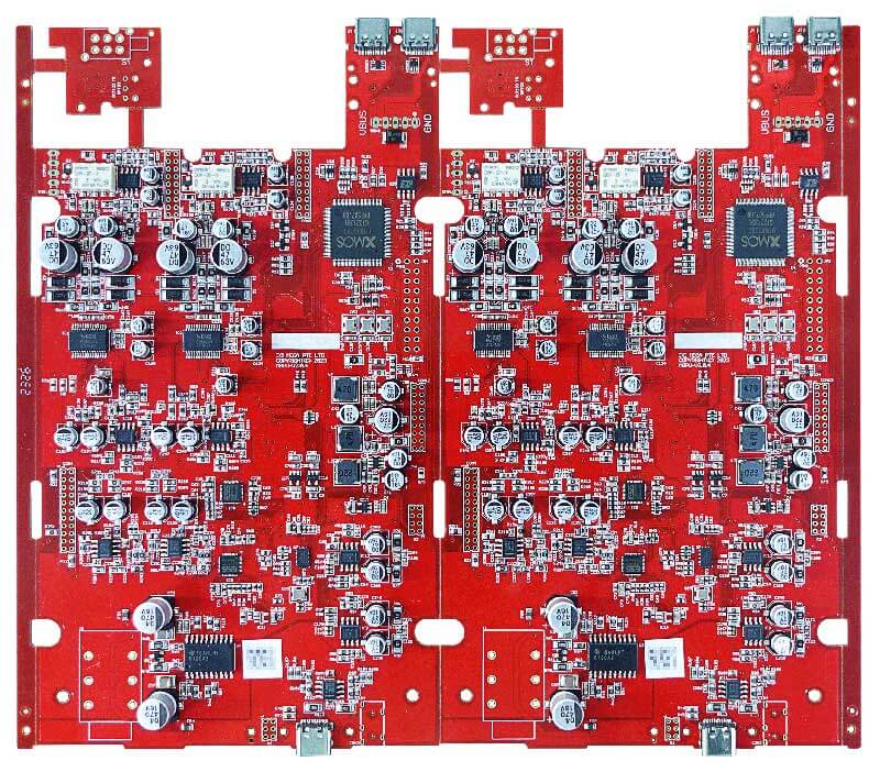
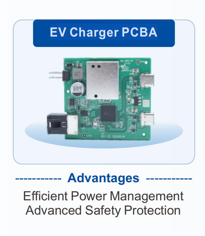
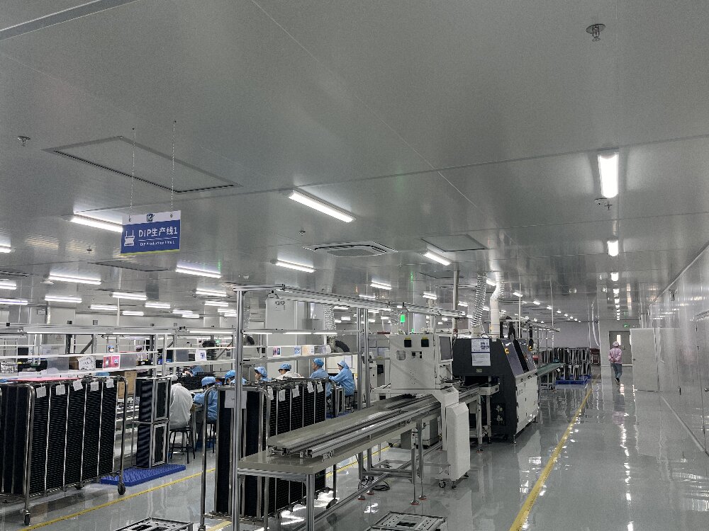
ICT (In-Circuit Test) is the most efficient method for detecting electrical defects in PCB assembly. By making contact with test points via a probe bed, ICT can verify the parameters of hundreds of components within a matter of seconds. This article analyses the principles, design and key implementation points of ICT.
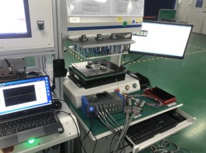
How ICT Works
ICT works by having probes make contact with test points on the PCB, applying a stimulus signal and measuring the response.
Test Capabilities: Measurement of resistance, capacitance and inductance; diode/transistor polarity and gain; IC pin open circuits/short circuits; and certain digital logic functions.
Test Speed: A typical board completes the full test in 30–60 seconds.

Probe Bed Fixture Structure
The probe bed is the hardware core of ICT.
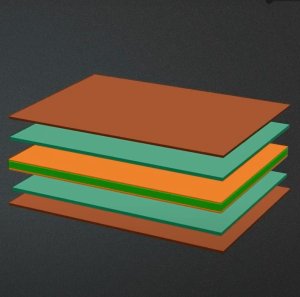
Structural components: probe board (made of acrylic or Delrin), probes (spring probes/pogo pins), positioning pins, clamping mechanism, and interface adapter board.
Probe selection: standard probes (100 mil pitch), fine-pitch probes (75 mil or 50 mil), and high-frequency probes (for signal integrity testing).
Test Point Design Rules
The accessibility of test points determines the ICT coverage.
Design rules: Diameter ≥ 0.8 mm (standard probes) or ≥ 0.5 mm (fine-pitch probes); distributed on a single side of the PCB; avoiding component bodies and obstructed areas; and at least one test point per network.
Coverage targets: ≥ 85% for general products; ≥ 95% for high-reliability products.
Boundary Scan (JTAG) Integration
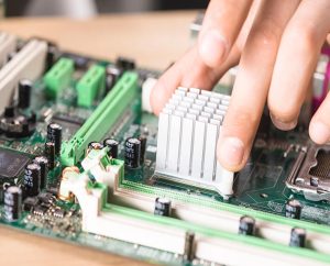
Traditional ICT struggles to cover high-density BGA boards.
Advantages of JTAG: Interconnection testing via the chip’s Test Access Port (TAP); no physical contact with internal nodes required; ability to test BGA solder joints for open circuits and short circuits; and support for In-System Programming (ISP).
Test Programme Development
The test programme determines the depth of ICT detection.
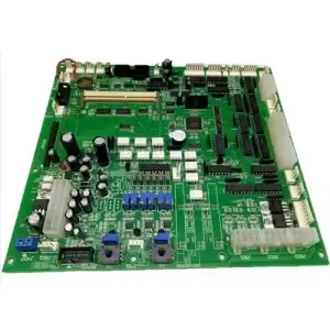
Development process: Import CAD data (Gerber, BOM, coordinates), generate the test point netlist, write test steps (using Guard technology to isolate parallel components), and perform debugging and validation.
Limitations of ICT
ICT is not a panacea and has the following limitations:
Cannot test functional performance (requires FCT as a supplement)
Cannot detect solder joint strength (requires X-ray or cross-section analysis)
Coverage is limited when there are insufficient test points
Fixture costs are high and lead times are long (typically 2–4 weeks for manufacture)
ICT is a crucial part of PCB assembly quality control. Planning the test point layout during the design phase and collaborating with factory test engineers can maximise the value of ICT.

Frequently Asked Questions (FAQ)
Q1: What is the difference between ICT and FCT?
A: ICT checks the parameters and connection integrity of individual components (manufacturing defects), whilst FCT verifies the functional performance of the entire circuit (design defects). ICT requires test points, whilst FCT requires functional fixtures and programmes. The two are complementary; typically, ICT is performed first to screen for obvious defects, followed by FCT to verify functionality.
Q2: Can ICT probes damage the PCB?
A: Not under normal use. Probe spring force is typically 100–200 g; the contact surface is plated with gold or rhodium and has a lower hardness than the pad. However, as probes wear, their tips become rough and may scratch the pads; they must therefore be replaced regularly (typically after 100,000 contacts). Designing test points to be concave or ring-shaped can reduce the risk of damage.
Q3: Can ICT be performed without test points?
A: Not with traditional ICT. Alternative options: 1) Use flying probe testing, which requires no fixture but is slow (10–30 minutes per board); 2) Increase boundary scan (JTAG) coverage; 3) Add test points during the Design for Testability (DFT) phase. The latter two options are significantly less costly than the former two.
Q4: How long is the lead time for manufacturing an ICT fixture?
A: Typically 2–4 weeks, depending on complexity and factory capacity. In urgent cases, this can be reduced to 1 week (with a 50–100 per cent rush charge). The fixture’s service life is approximately 50,000–100,000 press cycles, after which the probes must be replaced or the fixture completely rebuilt. For small-batch products, it is advisable to assess whether flying probe testing is more cost-effective.
Q5: Why does a product still fail even after passing ICT?
A: ICT only verifies the presence of components and the correctness of connections; it does not verify: 1) whether component functionality has failed (e.g. parameter drift in ICs damaged by ESD); 2) software issues; 3) timing issues; 4) analogue signal accuracy. These must be identified through FCT or system testing.
