


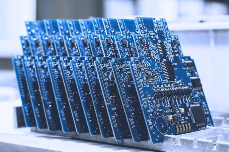
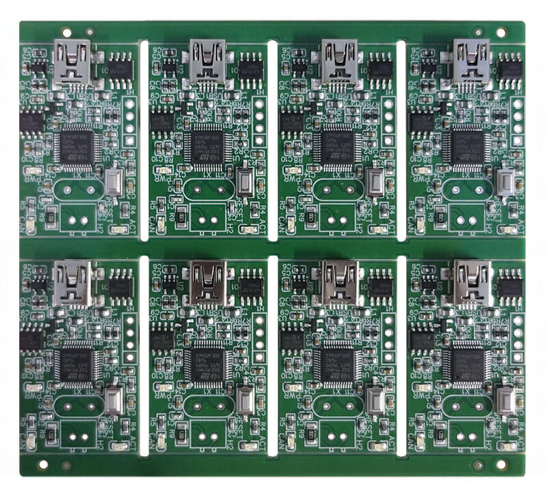
ESD (electrostatic discharge) is a momentary discharge phenomenon caused by the discharge of static electric charges between different potentials. It can generate high voltages and strong currents in an extremely short period of time, causing irreversible damage to electronic components on the PCB and even leading to the failure of the entire circuit board. Specific manifestations include short circuits or open circuits, signal integrity issues, and a shortened product lifespan. Therefore, ESD protection is crucial in PCB design, particularly in high-precision and multilayer designs, where proper protection measures can effectively enhance product reliability and durability.

The Impact and Hazards of ESD Damage on PCBs
ESD surges can cause solder joints to crack or components to fail, resulting in short circuits or open circuits that disrupt normal functionality. Additionally, ESD can interfere with signal transmission, leading to signal integrity issues such as bit errors and increased noise. Furthermore, cumulative ESD damage can cause product failure within a short period, significantly reducing the product’s service life. In high-precision and multilayer PCB designs, inadequate ESD protection directly affects product reliability and durability.
PCB Layout Optimization Is the Foundation of ESD Protection
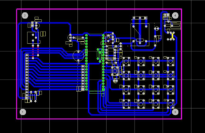
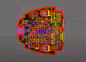
A well-designed PCB layout is the primary measure for reducing ESD damage. Placing ESD-sensitive components in the center of the PCB, away from the board edges, can effectively reduce the risk of direct electrostatic discharge. At the same time, the ground area should be increased to provide a larger ground plane, allowing static electricity to be rapidly dissipated to ground and reducing interference with electronic components. In terms of routing, signal lines and power lines must be kept at a sufficient distance to minimize electromagnetic interference and electrostatic coupling; in particular, high-speed signal routing should avoid proximity to board edges and high-potential areas.
Electrostatic Shielding Layers Enhance Protection
Electromagnetic shielding effectiveness can be enhanced through proper layer stacking design. Distributing power layers and ground planes across different PCB layers, and adding protective layers to the ground planes, can effectively reduce ESD propagation paths. At the same time, employing multi-point grounding and via connection designs allows static electricity to be routed to ground more rapidly, preventing its accumulation on the PCB surface and thereby improving overall shielding performance.
Key Considerations for Component Selection and Configuration
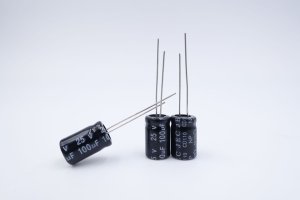
Installing Transient Voltage Suppressor (TVS) diodes in critical circuits and signal lines can rapidly absorb static electricity during an ESD event, protecting downstream components. Additionally, incorporating filtering components such as capacitors and inductors at the input and near sensitive devices can effectively reduce the risk of ESD energy entering sensitive circuits, thereby establishing a multi-level protection system.
Selection and Application of Anti-Static Materials
Using PCB materials with anti-static properties—such as polymer ESD protective coatings—forms a protective layer on the PCB surface to prevent static electricity buildup. At the same time, the appropriate use of copper cladding can effectively dissipate static electricity and reduce the impact of high-potential charges on components. The copper cladding layer must be connected to the ground plane so that static electricity can be discharged to ground more quickly.
ESD Testing and Validation Ensure Protection Reliability
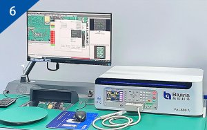
ESD testing and simulation experiments are conducted after PCB manufacturing is complete to ensure the boards can effectively protect against static electricity in practical applications. By analyzing test results, the PCB’s protective design is continuously optimized to improve the product’s ESD tolerance, thereby ensuring its reliability in real-world operating environments.
Conclusion
ESD protection is a critical aspect of PCB design that cannot be overlooked. By optimizing layout, adding electrostatic shielding layers, appropriately selecting protective components and anti-static materials, and conducting rigorous testing and validation, damage to circuit boards caused by electrostatic discharge can be effectively minimized. Incorporating ESD protection into the standardized PCB design process is a key measure for enhancing product reliability, extending service life, and ensuring signal integrity.
