The design and manufacture of a multilayer PCB can be overwhelming. Have you ever wondered how these intricate layers of circuits are put together to create powerful, compact electronic devices?
If you are finding difficulty in the process or encountering problems during custom PCB projects, you’ve got into the right place. This step-by-step description will help you understand the complications of the multilayer PCB manufacturing process. The whole process is broken down into simple and easy-to-understand procedures so that each step is easily understood.
So, let’s get started.
Understanding Multilayer PCBs
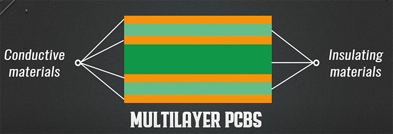
We all know that PCB acts as the backbone to connect and support most electronic components in almost every electronic device.
Generally, the substances used in the substrate are non-conductive, such as fiberglass; the conductive pathways are etched or printed onto it.
These paths allow the flow of electrical signals between components, thereby allowing the device’s functionality to operate.
Some of the multilayer PCBs achieve the concept when multiple layers of the conductive material are stacked and bonded together, leading to the most significant utilization of copper. Vias, small holes filled with conductive material, are used to interconnect different circuitry in every layer.
This layer stacking makes for more complex and compact board designs, meaning increased circuit density and functionality, without adding necessary physical size to the board.
From mobile phones, computers, and complex medical equipment to aeronautical progress and much more, multilayer PCBs have turned into a necessity in the world of modern electronic technology, where both space and performance heavily count.
Now you know the basics of multilayer PCBs, it’s time to learn how multilayer PCB is manufactured.
The Multilayer PCB Manufacturing Process
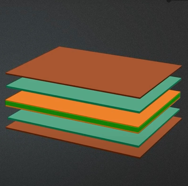
Creating a multilayer PCB involves several intricate and precise steps. Here’s a detailed breakdown of each stage in the manufacturing process:
1.Design and Layout
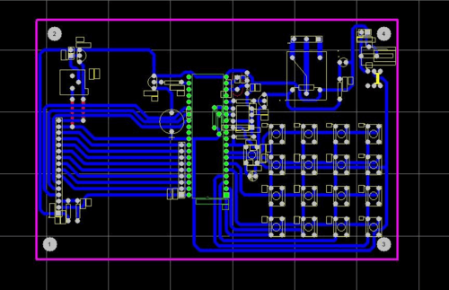
The first process in the manufacturing of a multilayer printed circuit board is board design. A designer makes the board or has a digital design data file with the circuit layout for each layer and interconnections.
To ensure there are no errors within the system and to boost efficiency during the design, designated software tools such as computer-aided design or CAD are used.
2.Material Selection
Material selection is regarded as being the most vital factor for the excellent performance and reliability of PCB. The primary material, selected FR4 or polyimide, for possessing dielectric properties or immortality during the process in manufacturing.
The core materials help electrically insulate the conductive layers and provide structural integrity to the PCB.
3.Inner Layer Fabrication
Inner layers are fabricated in a multi-step process, starting with developing the circuit patterns on separate layers. This is usually done through photolithography by coating the copper layer with a photoresist material and illuminating it with an ultraviolet source passed through a photomask.
The unmasked portions develop and, with a chemical etchant, seek to remove the copper, thereby “exposing” only the copper circuitry.
4.Core Drilling
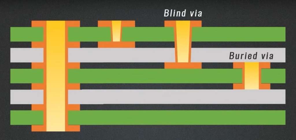
Once the inner layers are completed, you will have to drill very accurate holes through this core material. These holes are referred to as vias because they are used to make the eventual electrical connection between the various layers of the PCB.
Many highly developed drilling techniques will allow the generation of these holes with perfect accuracy of position and size.
5.Lamination
The further process is known as the lamination of layers and core material. The stack of layers is put in between high temperature and pressure. The alignment has to be exact because of the overlay of one layer over another.
The circuits printed on different layers will be interconnected precisely. The lamination makes a solid structure out of all the layers and core material.
6.Drilling
After the lamination of the layers, other kinds of holes are drilled through the entire pile. These will be component leads, among other connexions from the outer layers to the inner layers. This operation requires exact drilling machines.
7.Plating
The holes drilled in the board are plated along with the other outside surfaces using copper in the board plating process.
The most common technique is electroplating, in which the board is immersed in a solution of copper plating and then subjected to a regulated electric induction. This effectively forms a thin, uniform layer of copper that creates conductive paths between the layers.
8.Etching
Finally, the excess copper is etched away from the plated areas to define the final circuitry patterns on each layer. This is done by an etchant solution to dissolve unprotected copper, leaving only the intended circuitry.
9.Solder Mask Application
Next, a protective layer of solder mask is applied to the PCB. The solder mask covers the copper layer of the board, with selected areas around the component pins, vias, and pads exposed so that the component pin can be connected to the copper layer of the board through soldering.
This prevents short circuits and protects the copper traces from any corrosion.
10.Surface Finishing
A final protective layer is applied to enhance solderability and protect the exposed copper surfaces. Surface finishes can include ENIG for good solderability.
11.Electrical Testing
Afterward, the finished PCB circulates a series of rigorous electrical tests, guaranteeing that the interconnects are all running and ironing out any short circuits. Continuity and functionality are checked back, ensuring the board matches its specified design.
Assembly
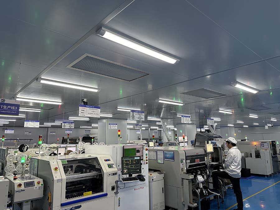
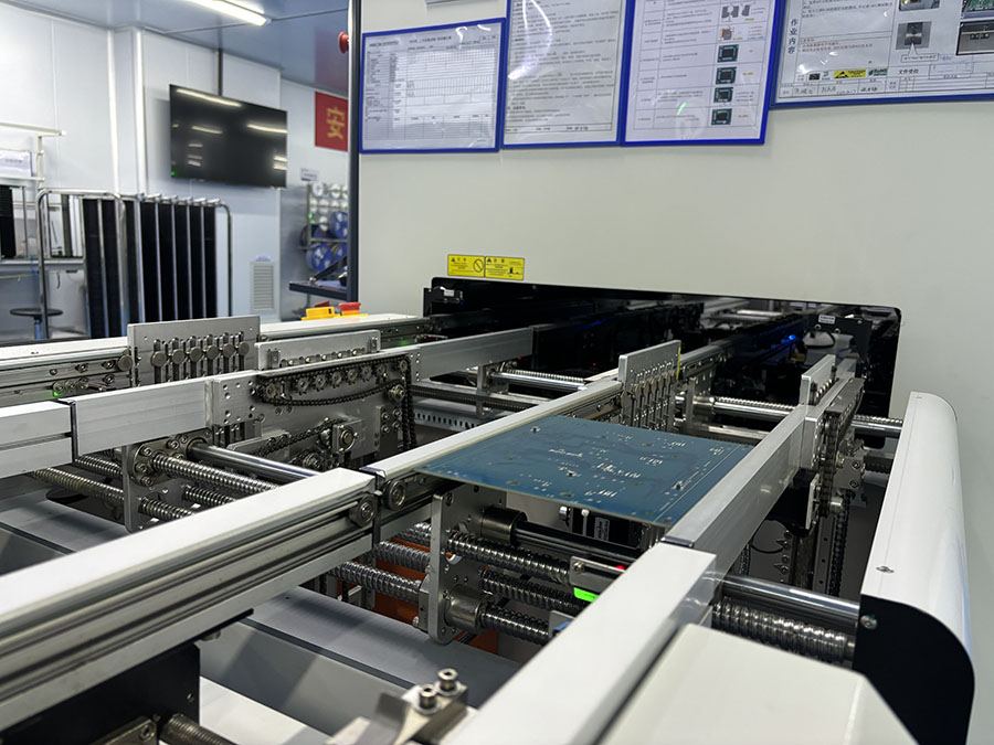
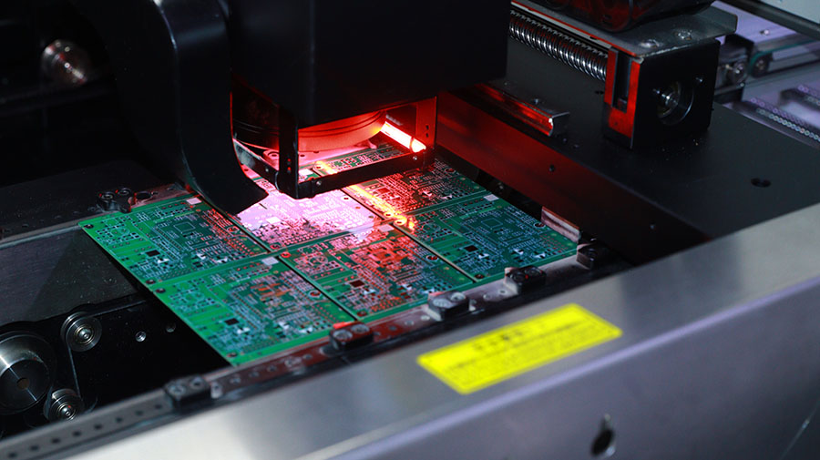
After the PCB is manufactured and tested, electronic components can be attached to the board. Once again, in assembly, this is most often done by soldering the components onto the exposed pads located on the PCB. SMT or surface mount technology and through-hole soldering are common ways use for assembly process.
Additional Design Considerations
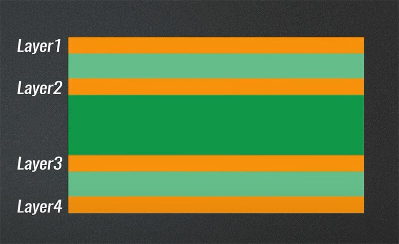
Here are some additional consideration for multilayer PCB manufacturing that you must know:
- Design for Manufacturability (DFM)
Design for Manufacturability (DFM) is a key practice in making multilayer PCBs. The key concepts and purposes observed by DFM concern that when implementing DFM principles in the early design stage to design boards that would not entail significant manufacturability problems before their production, most arising issues during the manufacturing process are avoidable.
Consequently, this will yield higher quality and improved yields, together with lower costs.
Also, DFM considers the layout of components and the spacing among them. Correctly placing components in a tight density reduces trace length and avoids convoluted routing, hence greatly easing the manufacturing process and optimizing a better design of the PCB relative to its performance and the reliability expected from it.
Proper trace width and spacing reduce electrical interference and increase the reliability of the circuit by always ensuring the connections. Ideally, the trace width and spacing should follow the industry standards to prevent defects from such design errors as shorts and opens.
Another thing essential to ensure is reducing the number of layers on the PCB. It can reduce manufacturing costs dramatically and also reduce intricacy. With optimization in routing and placements of components, the desired function can be provided with reduced layers.
Signal trace can lower layers if good signal quality is maintained with prudent planning. Signal integrity can be maintained using differential pair routing techniques, controlled impedance, etc.
- Quality Control
The quality control of multilayered PCBs is very important in assuring the final product meets required standards and, at the end of it all, performs reliably. This calls for strict quality control measures in every production phase to detect and fix any defects or deviations from specifications.
QC starts straight from the incoming material inspection. Materials such as copperclad laminates, solder resists, and core materials go through quality checks in line with the required specifications.
Unacceptable materials are rejected from those sources to avoid defects in the final product. While regular audits are one safeguard, good relations with suppliers insulate against fluctuations in material quality.
Process quality checks are implemented at different manufacturing stages. In fabricating the inner layers, checks are performed on pattern-transfer accuracy and proper etching. Through microscopic inspection, one can detect under-etching and over-etching.
The lamination of boards is checked for the correctness of alignment and integrity of bonding. Drilled holes are checked for cleanliness, correct position, and defects like burring.
- Cost and Lead Times
Understanding the factors that influence the cost and lead time of multilayer PCB manufacturing is crucial for effective project planning and budgeting. The two major primary factors he mentions are the number of layers and the complexity of a board. Increased layers mean increased materials, processing steps, killer ranges, and tighter tolerances, leading to increased costs.
Complex designs, which involve high-density wiring, large numbers of vias, and complex components, also take up much manufacturing time in sophisticated fabrication.
Material-based expenses are also important factors. Common materials like FR4 are both relatively cheap and common; on the other hand, advanced quality unique materials like polyimide or Rogers are far more expensive and, in many cases are ordered way ahead because of lack of availability.
There is also a cost component for board thickness and copper weight. Thicker board and heavier copper demand more raw material and processing time, raising the cost of material and manufacturing correspondingly.
Manufacturing processes themselves may also impact cost and lead time. Advanced techniques, like HDI, or High-Density Interconnect technology, typically including microvias and small line spacing, are more complex to do and cost more. A balance must be achieved between the demand for advanced features and manufacturability to control cost.
A high yield rate means the product has a low number of defects, yielding excellent efficiency in manufacturing and lowering the price. A low yield rate causes rework and scrap and may increase costs because of design or process problems.
Following these clearly defined stages will enable you to make multi-layered PCBs with present, stringent requirements for modern electronic gadgets in terms of reliability, performance, and compactness.
Conclusion
Multilayered PCB manufacturing appears complex initially, but understanding every single step lowers the complexity to manageable levels. Every stage, right from the very initial design and material selection to the very last assembly and quality checking, is instrumental in producing reliable and efficient PCBs.
This ensures the final product meets quality standards under challenging circumstances – for example, in today’s electronics that range from smartphones to advanced medical appliances.

