

Testing is where a PCBA design proves itself. A board that passes visual inspection may still contain open circuits, shorted traces, incorrect component values, or firmware programming errors that only manifest under specific conditions. At Keepbest, our test engineering team develops comprehensive validation strategies for every production program. This guide explains three advanced testing approaches — boundary scan, JTAG, and flying probe — along with when to specify each and how they fit into a comprehensive test strategy.
The Testing Hierarchy
Effective PCBA testing is layered. No single method catches every defect.
Visual and Automated Optical Inspection: AOI examines solder joints, component placement, polarity, and presence. It catches missing parts, reversed polarities, and obvious soldering defects. It cannot verify electrical function or hidden connections under BGA packages.
Solder Paste Inspection: SPI measures paste volume, height, and alignment before reflow. It prevents defects rather than detecting them after the fact. Boards with poor paste printing are reworked before components are placed.
In-Circuit Testing: ICT uses a bed-of-nails fixture to contact test points and verify component values, connectivity, and basic digital function. It requires test point access and dedicated fixturing. It is fast and comprehensive but expensive to set up for small volumes.
Functional Testing: The assembled board is powered and exercised through its operational modes. Functional testing validates the design rather than the manufacturing process. It requires custom test software and interface fixtures.
Advanced Methods: Boundary scan, JTAG, and flying probe fill gaps that traditional methods cannot address. They test digital interconnects, program devices, and verify complex boards without full test point coverage.
Boundary Scan Testing
Boundary scan is an IEEE 1149.1 standard methodology for testing digital interconnections on PCBAs without physical probe access. It relies on boundary scan cells built into compliant integrated circuits.
How It Works: Each boundary scan capable device contains a shift register adjacent to its I/O pins. In test mode, these registers disconnect the internal logic from the pins and allow the test controller to drive or sample pin states. By shifting patterns through the chain, the test system can verify connectivity between devices, detect opens and shorts, and even sample signals during normal operation.
The Boundary Scan Chain: Devices are connected in a serial chain from Test Data Input to Test Data Output. The chain is controlled by Test Clock and Test Mode Select signals. A compliant board may have one or multiple chains depending on device count and scan path optimization.
Defect Coverage: Boundary scan excels at detecting open solder joints on digital interconnections, shorted pins, stuck-at faults, and incorrect component orientation for scan-capable devices. It does not test analog circuits, power supplies, or non-scan components.
When to Specify: Boundary scan is essential for high-density boards with fine-pitch BGA and QFN packages where physical probe access is impossible. It is also valuable for boards with high digital complexity and limited test point real estate. Boundary scan requires that the design team implements 1149.1 compliance in the schematic and PCB layout, including chain routing and test access port connectors.
Coverage Enhancement: Boundary scan can be extended to test non-scan devices through gang testing or cluster testing. By controlling adjacent scan devices, the test system can drive signals into non-scan logic and measure responses through other scan pins. This extends coverage without adding full scan infrastructure to every device.
JTAG Testing and Programming
JTAG is often used interchangeably with boundary scan, but the distinction matters. JTAG is the physical interface standard. Boundary scan is one application of that interface.
The JTAG Interface: JTAG defines a four-wire protocol — Test Clock, Test Mode Select, Test Data Input, and Test Data Output — plus an optional Test Reset. These signals form a serial bus that can access internal test and debug resources on compliant devices.
Programming Applications: Modern microcontrollers, FPGAs, and CPLDs use JTAG for in-system programming. The manufacturing test system connects to the JTAG port, erases flash memory, writes firmware or configuration bitstreams, and verifies the programmed contents through readback. This eliminates the need for pre-programmed devices or socket programming.
Debug and Diagnostic Access: JTAG provides backdoor access to processor cores for debugging. During manufacturing, this enables diagnostic testing beyond simple pass-fail. Failed boards can be connected to a debug station through the JTAG port to identify the specific fault location and failure mode.
JTAG vs Traditional ICT: For boards with heavy BGA and fine-pitch component usage, JTAG-based testing can replace or supplement traditional ICT. JTAG requires no test point access to digital nets because the test data flows through the scan chain. This simplifies layout and reduces board size. However, JTAG alone cannot test analog circuits, power regulators, or discrete components.
Design for JTAG: To enable JTAG testing, the design must route the four JTAG signals to a dedicated connector or test point header. Chain topology must be verified for signal integrity at the intended test clock frequency. Device datasheets must be reviewed for compliance level, supported instructions, and boundary scan register length.
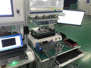
Flying Probe Testing
Flying probe testing uses automated mechanical probes that move across the board surface, contacting test points or component pads to perform electrical measurements without a fixed fixture.
How It Works: A flying probe machine contains four to eight independently movable probes mounted on precision linear drives. The probes contact specified test points under computer control, measuring resistance, capacitance, inductance, and voltage. The machine programs are generated from the PCB CAD data and component library.
Advantages Over ICT: Flying probe requires no test fixture, making it economical for prototypes and small batches. Setup time is hours rather than weeks. Test programs can be modified quickly as the design changes. Flying probe can access component pads directly, reducing the need for dedicated test points.
Limitations: Flying probe is slower than ICT because probes must physically move between measurements. A typical board may require several minutes of test time compared to seconds for an ICT fixture. Flying probe provides less power supply stress testing and limited digital functional coverage. High-volume production usually transitions to ICT or boundary scan once volumes justify fixture investment.
Modern Flying Probe Capabilities: Advanced flying probe systems now include JTAG integration, optical inspection, thermal testing, and even limited functional testing. Some systems can open and close switches on the board under test to isolate circuit segments. Laser-based microprobing allows contact with 50-micron pads without mechanical damage.
When to Specify Flying Probe: Flying probe is ideal for prototypes, NPI builds, and low-volume production where ICT fixturing is uneconomical. It is also useful for boards with severe test point access constraints where even boundary scan cannot achieve sufficient coverage. Many manufacturers use flying probe for first article inspection before committing to ICT fixture fabrication.

Comparing Test Methods
| Parameter | Boundary Scan | JTAG Programming | Flying Probe | ICT |
| — | — | — | — | — |
| Fixture required | No | No | No | Yes |
| Setup time | Low | Low | Low | High |
| Test speed | Fast | Moderate | Slow | Very fast |
| Digital coverage | Excellent | N/A | Limited | Good |
| Analog coverage | None | None | Moderate | Good |
| BGA/QFN access | Yes | Yes | Sometimes | Limited |
| Volume suitability | All | All | Low to medium | Medium to high |
| Design impact | Requires scan cells | Requires JTAG pins | Test points needed | Test points needed |
Integrating Test Strategy
A comprehensive test strategy combines multiple methods based on board characteristics and production volume.
Prototyping Phase: Use flying probe for electrical verification and JTAG for programming and boundary scan coverage. Add functional testing for design validation. No fixture investment is required at this stage.
NPI and Pilot Production: Evaluate whether ICT fixture investment is justified based on volume forecasts. If volumes exceed 1,000 units annually, ICT fixtures typically pay back within three to six months through reduced test time. Maintain flying probe for engineering builds and low-volume variants.
Volume Production: Deploy ICT for fast, comprehensive manufacturing verification. Use boundary scan for digital interconnects where ICT access is limited. Use JTAG for in-system programming. Add AOI and X-ray for process control. Functional testing remains the final gate before shipment.
Test Coverage Analysis: Calculate defect coverage by method and identify gaps. If analog circuits represent 30 percent of board area but only 10 percent of test coverage, supplement with functional testing or redesign for better test access. Target combined coverage above 95 percent for high-reliability products.
Cost Considerations
Test method selection has direct and indirect cost impacts.
Fixture Costs: ICT fixtures range from 2,000 to 15,000 dollars depending on probe count and complexity. Flying probe eliminates this cost but increases per-unit test time. For volumes under 500 units annually, flying probe is usually more economical.
Programming Costs: In-system programming through JTAG eliminates the cost of pre-programmed devices from distributors. However, programming time per board must be factored into line capacity. High-volume products may still benefit from factory-programmed devices to maximize throughput.
Rework and Scrap: Higher test coverage reduces field failures and warranty returns. The cost of a missed defect at the factory is typically 10 to 100 times higher when discovered in the field after assembly into a finished product. Investing in test coverage pays dividends in quality reputation.
Frequently Asked Questions
Q: Can boundary scan test analog components?
No. Boundary scan is designed for digital interconnect testing. Analog components must be tested through ICT, flying probe, or functional methods. The Keepbest test engineering team develops hybrid test strategies that combine boundary scan coverage for digital nets with targeted functional tests for analog circuits.
Q: Do all modern processors support JTAG?
Most ARM, RISC-V, and FPGA devices include JTAG or serial wire debug interfaces. However, implementation varies by manufacturer and device family. Always verify JTAG pin availability, supported debug protocols, and flash programming methods before committing to a design.
Q: How long does flying probe testing take per board?
Typical test times range from 2 to 10 minutes depending on test point count, measurement types, and probe movement optimization. Complex boards with hundreds of test points and mixed analog-digital measurements require longer. Flying probe is 10 to 50 times slower than ICT.
Q: Can I use flying probe for high-voltage or in-circuit functional testing?
Standard flying probe systems are limited to low-voltage measurements. Some advanced systems support power-up testing with limited voltage and current. For full functional testing under operating conditions, dedicated functional test fixtures are required.
Q: What is the minimum test point size for flying probe contact?
Most flying probe systems require test points or pads of at least 0.3 millimeters in diameter. Advanced systems with microprobing lasers can contact smaller pads. If test point access is severely constrained, boundary scan or redesign may be necessary.
Conclusion
No single test method catches every defect. Boundary scan solves access problems on dense digital boards. JTAG enables programming and diagnostic depth. Flying probe provides fixtureless flexibility for prototypes and low volumes. ICT delivers speed and comprehensiveness at scale. The optimal strategy layers these methods according to product complexity, volume, and quality requirements.
Contact the Keepbest test engineering team to review your design for testability. We will analyze your layout for test point coverage, evaluate boundary scan and JTAG feasibility, and propose a test strategy that balances coverage, cost, and throughput for your production volumes.